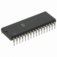
AT49F001N-70PI Atmel, AT49F001N-70PI Datasheet - Page 3

AT49F001N-70PI
Manufacturer Part Number
AT49F001N-70PI
Description
IC FLASH 1MBIT 70NS 32DIP
Manufacturer
Atmel
Datasheet
1.AT49F001-55VC.pdf
(22 pages)
Specifications of AT49F001N-70PI
Format - Memory
FLASH
Memory Type
FLASH
Memory Size
1M (128K x 8)
Speed
70ns
Interface
Parallel
Voltage - Supply
4.5 V ~ 5.5 V
Operating Temperature
-40°C ~ 85°C
Package / Case
32-DIP (0.600", 15.24mm)
Lead Free Status / RoHS Status
Contains lead / RoHS non-compliant
Other names
AT49F001N70PI
Device
Operation
1008D–FLASH–2/03
READ: The AT49F001(N)(T) is accessed like an EPROM. When CE and OE are low and WE
is high, the data stored at the memory location determined by the address pins is asserted on
the outputs. The outputs are put in the high impedance state whenever CE or OE is high. This
dual-line control gives designers flexibility in preventing bus contention.
COMMAND SEQUENCES: When the device is first powered on, it will be reset to the read or
standby mode depending upon the state of the control line inputs. In order to perform other
device functions, a series of command sequences are entered into the device. The command
sequences are shown in the Command Definitions table. The command sequences are written
by applying a low pulse on the WE or CE input with CE or WE low (respectively) and OE high.
The address is latched on the falling edge of CE or WE, whichever occurs last. The data is
latched by the first rising edge of CE or WE. Standard microprocessor write timings are used.
The address locations used in the command sequences are not affected by entering the com-
mand sequences.
RESET: A RESET input pin is provided to ease some system applications. When RESET is at
a logic high level, the device is in its standard operating mode. A low level on the RESET input
halts the present device operation and puts the outputs of the device in a high inpendance
state. If the RESET pin makes a high-to-low transition during a program or erase operation,
the operation may not be successfully completed and the operation will have to be repeated
after a high level is applied to the RESET pin. When a high level is reasserted on the RESET
pin, the device returns to the read or standby mode, depending upon the state of the control
inputs. By applying a 12V ± 0.5V input signal to the RESET pin, the boot block array can be
reprogrammed even if the boot block lockout feature has been enabled (see Boot Block Pro-
gramming Lockout Override section). The RESET feature is not available for the
AT49F001N(T).
ERASURE: Before a byte can be reprogrammed, the main memory block or parameter block
which contains the byte must be erased. The erased state of the memory bits is a logical “1”.
The entire device can be erased at one time by using a 6-byte software code. The software
chip erase code consists of 6-byte load commands to specific address locations with a specific
data pattern (please refer to the Chip Erase Cycle Waveforms).
After the software chip erase has been initiated, the device will internally time the erase opera-
tion so that no external clocks are required. The maximum time needed to erase the whole
chip is t
not be erased.
CHIP ERASE: If the boot block lockout has been enabled, the Chip Erase function will erase
Parameter Block 1, Parameter Block 2, Main Memory Block 1, and Main Memory Block 2 but
not the boot block. If the Boot Block Lockout has not been enabled, the Chip Erase function
will erase the entire chip. After the full chip erase the device will return back to read mode. Any
command during chip erase will be ignored.
EC
. If the boot block lockout feature has been enabled, the data in the boot sector will
AT49F001(N(T)
3


