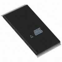
AT49F4096A-70TC Atmel, AT49F4096A-70TC Datasheet - Page 5

AT49F4096A-70TC
Manufacturer Part Number
AT49F4096A-70TC
Description
IC FLASH 4MBIT 70NS 48TSOP
Manufacturer
Atmel
Datasheet
1.AT49F4096A-90RI.pdf
(17 pages)
Specifications of AT49F4096A-70TC
Format - Memory
FLASH
Memory Type
FLASH
Memory Size
4M (512K x 8 or 256K x 16)
Speed
70ns
Interface
Parallel
Voltage - Supply
4.5 V ~ 5.5 V
Operating Temperature
0°C ~ 70°C
Package / Case
48-TSOP
Lead Free Status / RoHS Status
Contains lead / RoHS non-compliant
Available stocks
Company
Part Number
Manufacturer
Quantity
Price
Part Number:
AT49F4096A-70TC
Manufacturer:
ATMEL/爱特梅尔
Quantity:
20 000
AT49F4096A
BOOT BLOCK PROGRAMMING LOCKOUT OVERRIDE: The user can override the
boot block programming lockout by taking the RESET pin to 12 volts during the entire
chip erase, sector erase or word programming operation. When the RESET pin is
brought back to TTL levels, the boot block programming lockout feature is again active.
PRODUCT IDENTIFICATION: The product identification mode identifies the device and
manufacturer as Atmel. It may be accessed by hardware or software operation. The
hardware operation mode can be used by an external programmer to identify the correct
programming algorithm for the Atmel product.
For details, see “Operating Modes” (for hardware operation) or “Software Product Identi-
fication Entry/Exit” on page 13. The manufacturer and device codes are the same for
both modes.
DATA POLLING: The AT49F4096A features Data Polling to indicate the end of a pro-
gram cycle. During a program cycle, an attempted read of the last byte loaded will result
in the complement of the loaded data on I/O7. Once the program cycle has been com-
pleted, true data is valid on all outputs and the next cycle may begin. During a chip or
sector erase operation, an attempt to read the device will give a “0” on I/O7. Once the
program or erase cycle has completed, true data will be read from the device. Data Poll-
ing may begin at any time during the program cycle.
TOGGLE BIT: In addition to Data Polling, the AT49F4096A provides another method for
determining the end of a program or erase cycle. During a program or erase operation,
successive attempts to read data from the device will result in I/O6 toggling between
one and zero. Once the program cycle has completed, I/O6 will stop toggling and valid
data will be read. Examining the toggle bit may begin at any time during a program
cycle.
HARDWARE DATA PROTECTION: Hardware features protect against inadvertent pro-
grams to the AT49F4096A in the following ways: (a) V
sense: if V
is below 3.8V
CC
CC
(typical), the program function is inhibited. (b) V
power-on delay: once V
has
CC
CC
reached the V
sense level, the device will automatically time-out 10 ms (typical)
CC
before programming. (c) Program inhibit: holding any one of OE low, CE high or WE
high inhibits program cycles. (d) Noise filter: pulses of less than 15 ns (typical) on the
WE or CE inputs will not initiate a program cycle.
5
1604F–FLASH–4/04


