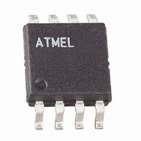
AT25256AW-10SI-2.7 Atmel, AT25256AW-10SI-2.7 Datasheet - Page 10

AT25256AW-10SI-2.7
Manufacturer Part Number
AT25256AW-10SI-2.7
Description
IC EEPROM 256KBIT 20MHZ 8SOIC
Manufacturer
Atmel
Datasheet
1.AT25128A-10PI-1.8.pdf
(24 pages)
Specifications of AT25256AW-10SI-2.7
Format - Memory
EEPROMs - Serial
Memory Type
EEPROM
Memory Size
256K (32K x 8)
Speed
10MHz, 20MHz
Interface
SPI, 3-Wire Serial
Voltage - Supply
2.7 V ~ 5.5 V
Operating Temperature
-40°C ~ 85°C
Package / Case
8-SOIC (5.3mm Width), 8-SOP, 8-SOEIAJ
Lead Free Status / RoHS Status
Contains lead / RoHS non-compliant
Other names
AT25256AW-10SI2.7
Available stocks
Company
Part Number
Manufacturer
Quantity
Price
Company:
Part Number:
AT25256AW-10SI-2.7
Manufacturer:
TI
Quantity:
4 500
10
AT25128A_256A
WRITE STATUS REGISTER (WRSR): The WRSR instruction allows the user to select one of
four levels of protection. The AT25128A/256A is divided into four array segments. Top quarter
(1/4), top half (1/2), or all of the memory segments can be protected. Any of the data within any
selected segment will therefore be read only. The block write protection levels and correspond-
ing status register control bits are shown in
The three bits, BP0, BP1, and WPEN are nonvolatile cells that have the same properties and
functions as the regular memory cells (e.g. WREN, t
Table 3-4.
The WRSR instruction also allows the user to enable or disable the write protect (WP) pin
through the use of the write protect enable (WPEN) bit. Hardware write protection is enabled
when the WP pin is low and the WPEN bit is “1”. Hardware write protection is disabled when
either the WP pin is high or the WPEN bit is “0”. When the device is hardware write protected,
writes to the Status Register, including the Block Protect bits and the WPEN bit, and the block-
protected sections in the memory array are disabled. Writes are only allowed to sections of the
memory which are not block-protected.
NOTE: When the WPEN bit is hardware write protected, it cannot be changed back to “0”, as
long as the WP pin is held low.
Table 3-5.
READ SEQUENCE (READ): Reading the AT25128A/256A via the SO pin requires the follow-
ing sequence. After the CS line is pulled low to select a device, the Read op-code is transmitted
via the SI line followed by the byte address to be read (see
pletion, any data on the SI line will be ignored. The data (D7 - D0) at the specified address is
then shifted out onto the SO line. If only one byte is to be read, the CS line should be driven high
after the data comes out. The read sequence can be continued since the byte address is auto-
matically incremented and data will continue to be shifted out. When the highest address is
WPEN
1(1/4)
2(1/2)
Level
3(All)
X
X
0
0
0
1
1
Block Write Protect Bits
WPEN Operation
High
High
Low
Low
WP
X
X
BP1
Status Register Bits
0
0
1
1
WEN
0
1
0
1
0
1
BP0
0
1
0
1
Protected
Protected
Protected
Protected
Protected
Protected
Protected
Blocks
Table
3-4.
3000 – 3FFF
2000 – 3FFF
0000 – 3FFF
AT25128A
WC
Array Addresses Protected
None
, RDSR).
Unprotected
Protected
Protected
Protected
Writable
Writable
Writable
Blocks
Table 3-6 on page
6000 – 7FFF
4000 – 7FFF
0000 – 7FFF
AT25256A
None
Protected
Protected
Protected
Protected
Register
Writable
Writable
Status
11). Upon com-
3368J–SEEPR–06/07


