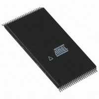
AT49BV320D-70TU Atmel, AT49BV320D-70TU Datasheet - Page 3

AT49BV320D-70TU
Manufacturer Part Number
AT49BV320D-70TU
Description
IC FLASH 32MBIT 70NS 48TSOP
Manufacturer
Atmel
Specifications of AT49BV320D-70TU
Format - Memory
FLASH
Memory Type
FLASH
Memory Size
32M (2M x 16)
Speed
70ns
Interface
Parallel
Voltage - Supply
2.65 V ~ 3.6 V
Operating Temperature
-40°C ~ 85°C
Package / Case
48-TSOP
Capacitance, Input
4 pF
Capacitance, Output
8 pF
Current, Input, Leakage
2 μA
Current, Output, Leakage
2
Density
32M
Organization
2M×16
Package Type
TSOP
Temperature, Operating
-40 to +85 °C
Time, Access
70 ns
Time, Address Setup
20
Voltage, Input, Low
0.6 V
Voltage, Output, Low
0.45 V
Voltage, Supply
2.65 to 3.6 V
Lead Free Status / RoHS Status
Lead free / RoHS Compliant
Available stocks
Company
Part Number
Manufacturer
Quantity
Price
Company:
Part Number:
AT49BV320D-70TU
Manufacturer:
ATMEL
Quantity:
5 530
Company:
Part Number:
AT49BV320D-70TU
Manufacturer:
ATMEL
Quantity:
6 250
Part Number:
AT49BV320D-70TU
Manufacturer:
ATMEL/爱特梅尔
Quantity:
20 000
3. Block Diagram
4. Device Operation
4.1
4.2
3581D–FLASH–2/06
A0 - A20
Command Sequences
Read
Y-DECODER
X-DECODER
ADDRESS
BUFFER
LATCH
INPUT
When the device is first powered on, it will be in the read mode. In order to perform other device
functions, a series of command sequences are entered into the device. The command
sequences are shown in the
inputs for the command codes). The command sequences are written by applying a low pulse
on the WE or CE input with CE or WE low (respectively) and OE high. The address and data are
latched by the first rising edge of CE or WE. Standard microprocessor write timings are used.
The address locations used in the command sequences are not affected by entering the com-
mand sequences.
When the AT49BV320D(T) is in the read mode, with CE and OE low and WE high, the data
stored at the memory location determined by the address pins are asserted on the outputs. The
OUTPUT
BUFFER
COMPARATOR
MEMORY
IDENTIFIER
I/O0 - I/O15
REGISTER
REGISTER
Y-GATING
STATUS
MAIN
DATA
“Command Definition Table” on page 15
BUFFER
INPUT
WRITE STATE
COMMAND
REGISTER
MACHINE
PROGRAM/ERASE
VOLTAGE SWITCH
AT49BV320D(T)
(I/O8 - I/O15 are don’t care
CE
WE
OE
RESET
WP
VPP
VCC
GND
3


