AT45DB321C-RU Atmel, AT45DB321C-RU Datasheet - Page 11
AT45DB321C-RU
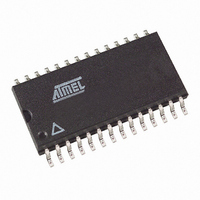
Manufacturer Part Number
AT45DB321C-RU
Description
IC FLASH 32MBIT 40MHZ 28SOIC
Manufacturer
Atmel
Datasheet
1.AT45DB321C-RU.pdf
(40 pages)
Specifications of AT45DB321C-RU
Format - Memory
FLASH
Memory Type
DataFLASH
Memory Size
32M (8192 pages x 528 bytes)
Speed
40MHz
Interface
SPI, 3-Wire Serial
Voltage - Supply
2.7 V ~ 3.6 V
Operating Temperature
-40°C ~ 85°C
Package / Case
28-SOIC (7.5mm Width)
Lead Free Status / RoHS Status
Lead free / RoHS Compliant
Available stocks
Company
Part Number
Manufacturer
Quantity
Price
Company:

Part Number:
AT45DB321C-RU
Manufacturer:
ATMEL
Quantity:
8
Part Number:
AT45DB321C-RU
Manufacturer:
ATMEL/爱特梅尔
Quantity:
20 000


6.3.1
6.3.2
6.3.3
3387M–DFLASH–2/08
Erasing the Sector Protection Register
Programming the Sector Protection Register
Reading the Sector Protection Register
To erase the Sector Protection Register, the CS pin must first be asserted. Once the CS pin has
been asserted, the 4-byte erase command sequence must be clocked in via the SI (serial input)
pin. After the last bit of the command sequence has been clocked in, the CS pin must be deas-
serted to initiate the internally self-timed erase cycle (t
that the device is busy during the erase cycle. The erased state of each bit (of a byte) in the Sec-
tor Protection Register indicates that the corresponding sector is flagged for protection. The
RESET pin is disabled during this erase cycle to prevent incomplete erasure of the Sector Pro-
tection Register.
To program the Sector Protection Register, the CS pin must first be asserted. Once the CS pin
has been asserted, the 4-byte command sequence must be clocked in via the SI (serial input)
pin. After the last bit of the command sequence has been clocked in, the data for the contents of
the Sector Protection Register must be clocked in. The first byte corresponds to sector 0 (0a,
0b), the second byte corresponds to Sector 1 and the last byte (byte 16) corresponds to Sector
15. After the last bit of data has been clocked in, the CS pin must be deasserted to initiate the
internally self-timed program cycle (t
busy during the program cycle. The RESET pin is disabled during this program cycle to prevent
incomplete programming of the sector protection register.
To read the Sector Protection Register, the CS pin must first be asserted. Once the CS pin has
been asserted, a 4-byte command sequence 32H, 00H, 00H, 00H and 32 don’t care clock cycles
must be clocked in via the SI (serial input) pin. The 32 don’t care clock cycles are required to ini-
tialize the read operation. After the 32 don’t care clock cycles, any additional clock pulses on the
SCK pin will result in data being output on the SO (serial output) pin. The read will begin with
Byte_1 of the Sector Protection Register for Sector_0, followed with Byte_2 for Sector_1. The
read operation will continue until Byte_16 for Sector_15 is read. Once the last byte is read a low-
to-high transition on the CS pin is required to terminate the read operation.
Note:
Command
Erase Sector Protection Register
Command
Program Sector Protection Register
Command
Read Sector Protection Register
Next generation devices of the “D” family will not require the 32 don’t care clock cycles.
P
). The Ready/Busy status will indicate that the device is
Byte 1
3DH
Byte 1
Byte 1
3DH
32H
PE
Byte 2
). The Ready/Busy status will indicate
2AH
Byte 2
Byte 2
2AH
00H
AT45DB321C
Byte 3
Byte 3
Byte 3
7FH
7FH
00H
Byte 4
Byte 4
Byte 4
CFH
FCH
00H
11
Related parts for AT45DB321C-RU
Image
Part Number
Description
Manufacturer
Datasheet
Request
R

Part Number:
Description:
DEV KIT FOR AVR/AVR32
Manufacturer:
Atmel
Datasheet:

Part Number:
Description:
INTERVAL AND WIPE/WASH WIPER CONTROL IC WITH DELAY
Manufacturer:
ATMEL Corporation
Datasheet:
Part Number:
Description:
Low-Voltage Voice-Switched IC for Hands-Free Operation
Manufacturer:
ATMEL Corporation
Datasheet:
Part Number:
Description:
MONOLITHIC INTEGRATED FEATUREPHONE CIRCUIT
Manufacturer:
ATMEL Corporation
Datasheet:
Part Number:
Description:
AM-FM Receiver IC U4255BM-M
Manufacturer:
ATMEL Corporation
Datasheet:
Part Number:
Description:
Monolithic Integrated Feature Phone Circuit
Manufacturer:
ATMEL Corporation
Datasheet:
Part Number:
Description:
Multistandard Video-IF and Quasi Parallel Sound Processing
Manufacturer:
ATMEL Corporation
Datasheet:
Part Number:
Description:
High-performance EE PLD
Manufacturer:
ATMEL Corporation
Datasheet:
Part Number:
Description:
8-bit Flash Microcontroller
Manufacturer:
ATMEL Corporation
Datasheet:
Part Number:
Description:
2-Wire Serial EEPROM
Manufacturer:
ATMEL Corporation
Datasheet: