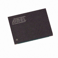
AT45DB321C-CI Atmel, AT45DB321C-CI Datasheet - Page 15

AT45DB321C-CI
Manufacturer Part Number
AT45DB321C-CI
Description
IC FLASH 32MBIT 40MHZ 24CBGA
Manufacturer
Atmel
Datasheet
1.AT45DB321C-RU.pdf
(40 pages)
Specifications of AT45DB321C-CI
Format - Memory
FLASH
Memory Type
DataFLASH
Memory Size
32M (8192 pages x 528 bytes)
Speed
40MHz
Interface
SPI, 3-Wire Serial
Voltage - Supply
2.7 V ~ 3.6 V
Operating Temperature
-40°C ~ 85°C
Package / Case
24-CBGA
Lead Free Status / RoHS Status
Contains lead / RoHS non-compliant
Available stocks
Company
Part Number
Manufacturer
Quantity
Price
7.4
7.4.1
7.4.2
7.4.3
7.4.4
7.4.5
3387M–DFLASH–2/08
Pin Descriptions
Serial Input (SI)
Serial Output (SO)
Serial Clock (SCK)
Chip Select (CS)
Write Protect (WP)
If a Group A mode is in progress (not fully completed), then another mode in Group A should not
be started. However, during this time in which a Group A mode is in progress, modes in Group B
can be started, except the first two Group A commands (Memory Array Read Commands).
This gives the DataFlash the ability to virtually accommodate a continuous data stream. While
data is being programmed into main memory from buffer 1, data can be loaded into buffer 2 (or
vice versa). See application note AN-4 (“Using Atmel’s Serial DataFlash”) for more details.
The SI pin is an input-only pin and is used to shift data serially into the device. The SI pin is used
for all data input, including opcodes and address sequences.
The SO pin is an output-only pin and is used to shift data serially out from the device.
The SCK pin is an input-only pin and is used to control the flow of data to and from the
DataFlash. Data is always clocked into the device on the rising edge of SCK and clocked out of
the device on the falling edge of SCK.
The DataFlash is selected when the CS pin is low. When the device is not selected, data will not
be accepted on the input pin (SI), and the output pin (SO) will remain in a high impedance state.
A high-to-low transition on the CS pin is required to start an operation, and a low-to-high transi-
tion on the CS pin is required to end an operation or to start an internally self-timed operation.
The WP pin is used to control the Hardware Sector Protection. Hardware Sector Protection is
enabled by asserting the WP pin and keeping the pin in it’s asserted state. Disabling Hardware
Sector Protection is accomplished by simply deasserting the WP pin. The WP pin will override
the software controlled sector protection method but only for protecting the sectors. For exam-
ple, if the sectors were not previously protected by the Enable Sector Protection command, then
simply asserting the WP pin for the minimum specified time (t
tection. When the WP pin is deasserted; however, the sector protection would no longer be
enabled as long as the Enable Sector Protection command was not issued while the WP pin was
asserted. If the Enable Sector Protection command was issued before or while the WP pin was
asserted, then simply deasserting the WP pin would not disable the sector protection. In this
case, the Disable Sector Protection command would need to be issued while the WP pin is
deasserted to disable the sector protection. The Disable Sector Protection command is also
ignored whenever the WP pin is asserted.
To ensure backwards compatibility with previous generations of DataFlash, the function of the
WP pin has not changed. Therefore, when the WP pin is asserted, certain sectors in the memory
array will be protected, and when the WP pin is deasserted, the memory array will be unpro-
tected provided the Enable Sector Protection command hasn’t been issued. New devices are
shipped from Atmel with the contents of the Sector Protection Register pre-programmed with
“00H” (unprotect). The user can reprogram the Sector Protection Register to change which sec-
tors will be protected by the WP pin.
WPE
) would enable the sector pro-
AT45DB321C
15


