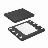
AT45DB021D-MH-Y Atmel, AT45DB021D-MH-Y Datasheet - Page 28

AT45DB021D-MH-Y
Manufacturer Part Number
AT45DB021D-MH-Y
Description
IC FLASH 2MBIT 66MHZ 8UDFN
Manufacturer
Atmel
Datasheet
1.AT45DB021D-SH-T.pdf
(48 pages)
Specifications of AT45DB021D-MH-Y
Format - Memory
FLASH
Memory Type
DataFLASH
Memory Size
2M (1024 pages x 264 bytes)
Speed
66MHz
Interface
SPI, RapidS
Voltage - Supply
2.7 V ~ 3.6 V
Operating Temperature
-40°C ~ 85°C
Package / Case
8-UDFN
Architecture
Sectored
Interface Type
SPI Serial
Supply Voltage (max)
3.6 V
Supply Voltage (min)
2.7 V
Maximum Operating Current
15 mA
Mounting Style
SMD/SMT
Organization
32 KB x 8
Lead Free Status / RoHS Status
Lead free / RoHS Compliant
Other names
AT45DB021D-MH
AT45DB021D-MH
AT45DB021D-MU
AT45DB021D-MU
AT45DB021D-MH
AT45DB021D-MU
AT45DB021D-MU
14.
14.1
15.
28
Power-on/Reset State
When power is first applied to the device, or when recovering from a reset condition, the device will default to Mode
3. In addition, the output pin (SO) will be in a high impedance state, and a high-to-low transition on the CS pin will
be required to start a valid instruction. The mode (Mode 3 or Mode 0) will be automatically selected on every falling
edge of CS by sampling the inactive clock state.
Initial Power-up/Reset Timing Restrictions
At power up, the device must not be selected until the supply voltage reaches the V
t
above the Power-on Reset threshold value (V
respond to any commands. After power up is applied and the V
the t
Similarly, the t
device can perform a write (Program or Erase) operation. After initial power-up, the device will default in Standby
mode.
Table 14-1.
System Considerations
The serial interface is controlled by the clock SCK, serial input SI and chip select CS pins. These signals must rise
and fall monotonically and be free from noise. Excessive noise or ringing on these pins can be misinterpreted as
multiple edges and cause improper operation of the device. The PC board traces must be kept to a minimum
distance or appropriately terminated to ensure proper operation. If necessary, decoupling capacitors can be added
on these pins to provide filtering against noise glitches.
As system complexity continues to increase, voltage regulation is becoming more important. A key element of any
voltage regulation scheme is its current sourcing capability. Like all Flash memories, the peak current for Atmel
DataFlash
requirement. An under specified regulator can cause current starvation. Besides increasing system noise, current
starvation during programming or erase can lead to improper operation and possible data corruption.
In an effort to continue our goal of maintaining world-class quality leadership, Atmel has been performing extensive
testing on the Atmel AT45DB021D that would not normally be done with a Serial Flash device. The testing that has
been performed on the AT45DB021D involved extensive, non-stop reading of the memory array on pre-
conditioned devices. The pre-conditioning of the devices, which entailed erasing and programming the entire
memory array 10,000 times, was done to simulate a customer environment and to exercise the memory cells to a
certain degree. The non-stop reading of the devices was done in three levels of granularity, with the first level
involving a continuous, looped read of 256-bytes (a single page) of memory, the second level involving a
continuous, looped-read of a 4-Kbyte (16-pages) portion of memory, and the third level entailing non-stop reading
of the entire memory array. Read operations were performed at both +25°C and +125°C and with a supply voltage
of 3.7V, which exceeds the specified datasheet operating voltage range. The results of all of the extensive tests
indicate that the contents of a portion of memory being read continuously could be altered after 800,000,000 read
operations only if that portion of the memory was not erased or reprogrammed at all during the 800,000,000 read
operations. If that portion of memory was reprogrammed at some point, then it would take another 800,000,000
VCSL
Symbol
t
t
V
Atmel AT45DB021D
VCSL
PUW
POR
VCSL
. During power-up, the internal Power-on Reset circuitry keeps the device in reset mode until the V
delay is required before the device can be selected in order to perform a read operation.
®
occur during the programming and erase operation. The regulator needs to supply this peak current
Parameter
V
Power-Up Device Delay before Write Allowed
Power-On Reset Voltage
CC
PUW
Initial Power-up/Reset Timing Restrictions
(min.) to Chip Select low
delay is required after the V
POR
CC
rises above the Power-on Reset threshold value (V
). At this time, all operations are disabled and the device does not
Min
1.5
1
CC
is at the minimum operating voltage V
Typ
Max
2.5
20
CC
(min.) and further delay of
Units
ms
ms
V
3638J–DFLASH–5/10
POR
) before the
CC
CC
(min.),
rises
®


