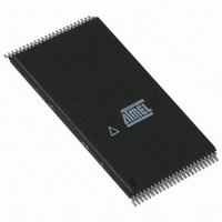
AT49BV802D-70TU Atmel, AT49BV802D-70TU Datasheet - Page 19

AT49BV802D-70TU
Manufacturer Part Number
AT49BV802D-70TU
Description
IC FLASH 8MBIT 70NS 48TSOP
Manufacturer
Atmel
Specifications of AT49BV802D-70TU
Format - Memory
FLASH
Memory Type
FLASH
Memory Size
8M (512K x 16)
Speed
70ns
Interface
Parallel
Voltage - Supply
2.65 V ~ 3.6 V
Operating Temperature
-40°C ~ 85°C
Package / Case
48-TSOP
Capacitance, Input
4 pF
Capacitance, Output
8 pF
Current, Input, Leakage
2 μA
Current, Operating
2 μA
Current, Output, Leakage
2
Density
8M
Organization
512K×16
Package Type
TSOP
Temperature, Operating
-40 to +85 °C
Time, Access
70 ns
Time, Address Hold
25
Voltage, Input, High
2 V
Voltage, Input, Low
0.6 V
Voltage, Output, High
2.5 V
Voltage, Output, Low
0.45 V
Voltage, Supply
2.65 to 3.6 V
Lead Free Status / RoHS Status
Lead free / RoHS Compliant
Available stocks
Company
Part Number
Manufacturer
Quantity
Price
14. AC Read Characteristics
15. AC Read Waveforms
Notes:
3626A–FLASH–2/07
Symbol
t
t
t
t
t
t
t
RC
ACC
CE
OE
DF
OH
RO
(1)
(3)(4)
(2)
1. CE may be delayed up to t
2. OE may be delayed up to t
3. t
4. This parameter is characterized and is not 100% tested.
without impact on t
DF
is specified from OE or CE, whichever occurs first (CL = 5 pF).
Parameter
Read Cycle Time
Address to Output Delay
CE to Output Delay
OE to Output Delay
CE or OE to Output Float
Output Hold from OE, CE or Address,
whichever occurred first
RESET to Output Delay
RESET
ACC
OUTPUT
ADDRESS
CE
OE
.
ACC
CE
(1)(2)(3)(4)
- t
- t
OE
CE
after the falling edge of CE without impact on t
after the address transition without impact on t
HIGH Z
t
ACC
t
RO
ADDRESS VALID
t
CE
t
OE
t
RC
OUTPUT
VALID
Min
70
0
0
0
AT49BV802D(T)-70
t
OH
t
DF
CE
ACC
or by t
.
ACC
AT49BV802D(T)
Max
100
70
70
20
25
- t
OE
after an address change
Units
ns
ns
ns
ns
ns
ns
ns
19


