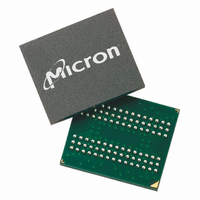
MT48H8M32LFB5-75:G TR Micron Technology Inc, MT48H8M32LFB5-75:G TR Datasheet - Page 56

MT48H8M32LFB5-75:G TR
Manufacturer Part Number
MT48H8M32LFB5-75:G TR
Description
IC SDRAM 256MBIT 132MHZ 90VFBGA
Manufacturer
Micron Technology Inc
Type
Mobile SDRAMr
Specifications of MT48H8M32LFB5-75:G TR
Format - Memory
RAM
Memory Type
Mobile SDRAM
Memory Size
256M (8Mx32)
Speed
132MHz
Interface
Parallel
Voltage - Supply
1.7 V ~ 1.95 V
Operating Temperature
0°C ~ 70°C
Package / Case
90-VFBGA
Organization
8Mx32
Density
256Mb
Address Bus
14b
Access Time (max)
8/6ns
Maximum Clock Rate
133MHz
Operating Supply Voltage (typ)
1.8V
Package Type
VFBGA
Operating Temp Range
0C to 70C
Operating Supply Voltage (max)
1.95V
Operating Supply Voltage (min)
1.7V
Supply Current
100mA
Pin Count
90
Mounting
Surface Mount
Operating Temperature Classification
Commercial
Lead Free Status / RoHS Status
Lead free / RoHS Compliant
Other names
557-1328-2
WRITE Operation
Figure 26: WRITE Burst
PDF: 09005aef834c13d2
256mb_mobile_sdram_y36n.pdf - Rev. I 11/09 EN
Note:
WRITE bursts are initiated with a WRITE command, as shown in Figure 10 (page 30).
The starting column and bank addresses are provided with the WRITE command and
auto precharge is either enabled or disabled for that access. If auto precharge is ena-
bled, the row being accessed is precharged at the completion of the burst. For the
generic WRITE commands used in the following figures, auto precharge is disabled.
During WRITE bursts, the first valid data-in element is registered coincident with the
WRITE command. Subsequent data elements are registered on each successive positive
clock edge. Upon completion of a fixed-length burst, assuming no other commands
have been initiated, the DQ will remain at High-Z and any additional input data will be
ignored (see Figure 26 (page 56)). A continuous page burst continues until termina-
ted; at the end of the page, it wraps to column 0 and continues.
Data for any WRITE burst can be truncated with a subsequent WRITE command, and
data for a fixed-length WRITE burst can be followed immediately by data for a WRITE
command. The new WRITE command can be issued on any clock following the previ-
ous WRITE command, and the data provided coincident with the new command ap-
plies to the new command (see Figure 27 (page 57)). Data n + 1 is either the last of a
burst of two or the last desired data element of a longer burst.
Mobile LPSDR devices use a pipelined architecture and therefore do not require the 2n
rule associated with a prefetch architecture. A WRITE command can be initiated on any
clock cycle following a previous WRITE command. Full-speed random write accesses
within a page can be performed to the same bank, as shown in Figure 28 (page 58), or
each subsequent WRITE can be performed to a different bank.
Command
Address
1. BL = 2. DQM is LOW.
CLK
DQ
WRITE
Bank,
Col n
T0
D
IN
Transitioning data
NOP
256Mb: 16 Meg x 16, 8 Meg x 32 Mobile SDRAM
T1
D
IN
56
NOP
T2
Don’t Care
Micron Technology, Inc. reserves the right to change products or specifications without notice.
T3
NOP
©2008 Micron Technology, Inc. All rights reserved.
WRITE Operation


