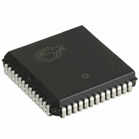
CY7C146-25JC Cypress Semiconductor Corp, CY7C146-25JC Datasheet - Page 7

CY7C146-25JC
Manufacturer Part Number
CY7C146-25JC
Description
IC SRAM 16KBIT 25NS 52PLCC
Manufacturer
Cypress Semiconductor Corp
Specifications of CY7C146-25JC
Format - Memory
RAM
Memory Type
SRAM - Dual Port, Asynchronous
Memory Size
16K (2K x 8)
Speed
25ns
Interface
Parallel
Voltage - Supply
4.5 V ~ 5.5 V
Operating Temperature
0°C ~ 70°C
Package / Case
52-PLCC
Density
16Kb
Access Time (max)
25ns
Sync/async
Asynchronous
Architecture
SDR
Clock Freq (max)
Not RequiredMHz
Operating Supply Voltage (typ)
5V
Address Bus
22b
Package Type
PLCC
Operating Temp Range
0C to 70C
Number Of Ports
2
Supply Current
170mA
Operating Supply Voltage (min)
4.5V
Operating Supply Voltage (max)
5.5V
Operating Temperature Classification
Commercial
Mounting
Surface Mount
Pin Count
52
Word Size
8b
Number Of Words
2K
Lead Free Status / RoHS Status
Contains lead / RoHS non-compliant
Other names
428-1202
Available stocks
Company
Part Number
Manufacturer
Quantity
Price
Company:
Part Number:
CY7C146-25JC
Manufacturer:
CYPRESS
Quantity:
1 980
Company:
Part Number:
CY7C146-25JC
Manufacturer:
CY
Quantity:
426
Company:
Part Number:
CY7C146-25JC
Manufacturer:
Cypress Semiconductor Corp
Quantity:
10 000
Part Number:
CY7C146-25JC
Manufacturer:
CYPRESS/赛普拉斯
Quantity:
20 000
Switching Characteristics
Over the Operating Range (Speeds -35, -45, -55)
Switching Waveforms
Notes
Document #: 38-06031 Rev. *E
Interrupt Timing
t
t
t
t
t
t
17. R/W is HIGH for read cycle.
18. Device is continuously selected, CE = V
19. Address valid prior to or coincident with CE transition LOW.
WINS
EINS
INS
OINR
EINR
INR
Parameter
DATA OUT
ADDRESS
DATA OUT
I
CE
OE
CC
I
SB
R/W to INTERRUPT Set Time
CE to INTERRUPT Set Time
Address to INTERRUPT Set Time
OE to INTERRUPT Reset Time
CE to INTERRUPT Reset Time
Address to INTERRUPT Reset Time
[16]
PREVIOUS DATA VALID
t
PU
t
LZCE
t
OHA
Figure 4. Read Cycle No. 1 (Either Port-Address Access)
Description
IL
and OE = V
Figure 5. Read Cycle No. 2 (Either Port-CE/OE )
t
LZOE
t
ACE
IL
.
[13]
[13]
[8]
t
DOE
(continued)
[13]
t
AA
t
RC
Min
7C132-35
7C136-35
7C142-35
7C146-35
Max
25
25
25
25
25
25
DATA VALID
CY7C136A, CY7C142, CY7C146
Min
7C132-45
7C136-45
7C142-45
7C146-45
[17, 19]
t
HZOE
DATA VALID
[17, 18]
Max
35
35
35
35
35
35
CY7C132, CY7C136
t
HZCE
t
Min
PD
7C136A-55
7C132-55
7C136-55
7C142-55
7C146-55
Max
45
45
45
45
45
45
Page 7 of 15
Unit
ns
ns
ns
ns
ns
ns
[+] Feedback


