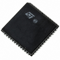
PSD813F1A-12JI STMicroelectronics, PSD813F1A-12JI Datasheet - Page 57

PSD813F1A-12JI
Manufacturer Part Number
PSD813F1A-12JI
Description
IC FLASH 1MBIT 120NS 52PLCC
Manufacturer
STMicroelectronics
Datasheet
1.PSD813F1A-90U.pdf
(111 pages)
Specifications of PSD813F1A-12JI
Format - Memory
FLASH
Memory Type
FLASH
Memory Size
1M (128K x 8)
Speed
120ns
Interface
Parallel
Voltage - Supply
4.5 V ~ 5.5 V
Operating Temperature
-40°C ~ 85°C
Package / Case
52-PLCC
Lead Free Status / RoHS Status
Contains lead / RoHS non-compliant
Other names
497-1973-5
Available stocks
Company
Part Number
Manufacturer
Quantity
Price
Company:
Part Number:
PSD813F1A-12JI
Manufacturer:
STMicroelectronics
Quantity:
10 000
JTAG In-System Programming (ISP)
Port C is JTAG compliant, and can be used for In-
System Programming (ISP). You can multiplex
JTAG operations with other functions on Port C
because ISP is not performed during normal sys-
tem operation. For more information on the JTAG
Port, see the section entitled
CIRCUIT
INTERFACE, page
Port Configuration Registers (PCR)
Each Port has a set of Port Configuration Regis-
ters (PCR) used for configuration. The contents of
the registers can be accessed by the MCU through
normal READ/WRITE bus cycles at the addresses
given in
ble 6., page 17
the base of the CSIOP register.
Table 6., page
USING
are the offsets in hexadecimal from
71.
THE
17. The addresses in
PROGRAMMING IN-
JTAG
SERIAL
Ta-
The pins of a port are individually configurable and
each bit in the register controls its respective pin.
For example, Bit 0 in a register refers to Bit 0 of its
port. The three Port Configuration Registers
(PCR), shown in Table 22, are used for setting the
Port configurations. The default Power-up state for
each register in Table
Control Register
Any bit reset to ‘0’ in the Control Register sets the
corresponding port pin to MCU I/O Mode, and a ‘1’
sets it to Address Out Mode. The default mode is
MCU I/O. Only Ports A and B have an associated
Control Register.
Table 22. Port Configuration Registers (PCR)
Note: 1. See
Control
Direction
Drive Select
Register Name
Table 26., page 58
1
A,B
A,B,C,D
A,B,C,D
22
Port
for Drive Register bit definition.
is 00h.
WRITE/READ
WRITE/READ
WRITE/READ
PSD813F1A
MCU Access
57/111


