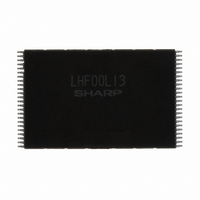
LHF00L13 Sharp Microelectronics, LHF00L13 Datasheet - Page 7

LHF00L13
Manufacturer Part Number
LHF00L13
Description
IC FLASH 32MBIT 90NS 48TSOP
Manufacturer
Sharp Microelectronics
Datasheet
1.LHF00L13.pdf
(40 pages)
Specifications of LHF00L13
Format - Memory
FLASH
Memory Type
FLASH
Memory Size
32M (2M x 16)
Speed
90ns
Interface
Parallel
Voltage - Supply
2.7 V ~ 3.6 V
Operating Temperature
-40°C ~ 85°C
Package / Case
48-TSOP
Lead Free Status / RoHS Status
Lead free / RoHS Compliant
Other names
425-1882
DQ
Symbol
A
RST#
V
GND
WE#
WP#
OE#
CE#
V
V
20
15
NC
CCQ
CC
PP
-A
-DQ
0
0
INPUT/SUPPLY
OUTPUT
SUPPLY
SUPPLY
SUPPLY
INPUT/
INPUT
INPUT
INPUT
INPUT
INPUT
INPUT
Type
ADDRESS INPUTS: Inputs for addresses.
DATA INPUTS/OUTPUTS: Inputs data and commands during CUI (Command User
Interface) write cycles, outputs data during memory array, status register, query code,
identifier code reads. Data pins float to high-impedance (High Z) when the chip or
outputs are deselected. Data is internally latched during an erase or program cycle.
CHIP ENABLE: Activates the device’s control logic, input buffers, decoders and sense
amplifiers. CE#-high (V
standby levels.
RESET: When low (V
which provides data protection. RST#-high (V
power-up or reset mode, the device is automatically set to read array mode. RST# must
be low during power-up/down.
OUTPUT ENABLE: Gates the device’s outputs during a read cycle.
WRITE ENABLE: Controls writes to the CUI and array blocks. Addresses and data are
latched on the rising edge of CE# or WE# (whichever goes high first).
WRITE PROTECT: When WP# is V
or program operation can be executed to the blocks which are not locked and not locked-
down. When WP# is V
MONITORING POWER SUPPLY VOLTAGE: V
With V
executed and should not be attempted.
Applying 12.0V±0.3V to V
mode, V
only be done for a maximum of 1,000 cycles on each block. V
12.0V±0.3V for a total of 80 hours maximum. Use of this pin at 12.0V+0.3V beyond
these limits may reduce block cycling capability or cause permanent damage.
DEVICE POWER SUPPLY (2.7V-3.6V): With V
flash memory are inhibited. Device operations at invalid V
Characteristics) produce spurious results and should not be attempted.
INPUT/OUTPUT POWER SUPPLY (2.7V-3.6V): Power supply for all input/output
pins.
GROUND: Do not float any ground pins.
NO CONNECT: Lead is not internally connected; it may be driven or floated.
PP
PP
≤V
is power supply pin. Applying 12.0V±0.3V to V
PPLK
Table 1. Pin Descriptions
, block erase, full chip erase, program or OTP program cannot be
LHF00L13
IL
IH
), RST# resets internal automation and inhibits write operations
, lock-down is disabled.
IH
) deselects the device and reduces power consumption to
PP
provides fast erasing or fast programming mode. In this
Name and Function
IL
, locked-down blocks cannot be unlocked. Erase
IH
PP
CC
) enables normal operation. After
is not used for power supply pin.
≤V
LKO
PP
, all write attempts to the
during erase/program can
PP
CC
may be connected to
voltage (see DC
Rev. 2.45
4


