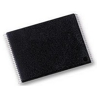
NAND256W3A2BN6E NUMONYX, NAND256W3A2BN6E Datasheet - Page 6

NAND256W3A2BN6E
Manufacturer Part Number
NAND256W3A2BN6E
Description
IC FLASH 256MBIT 48TSOP
Manufacturer
NUMONYX
Datasheet
1.NAND128W3A2BN6E.pdf
(59 pages)
Specifications of NAND256W3A2BN6E
Format - Memory
FLASH
Memory Type
FLASH - Nand
Memory Size
256M (32M x 8)
Interface
Parallel
Voltage - Supply
2.7 V ~ 3.6 V
Operating Temperature
-40°C ~ 85°C
Package / Case
48-TSOP
Access Time
12µs
Supply Voltage Range
1.7V To 1.95V, 2.7V To 3.6V
Memory Case Style
TSOP
No. Of Pins
48
Base Number
256
Block Size
16896Byte
Memory Configuration
32k X 8
Rohs Compliant
Yes
Lead Free Status / RoHS Status
Lead free / RoHS Compliant
Speed
-
Lead Free Status / RoHS Status
Lead free / RoHS Compliant, Lead free / RoHS Compliant
Other names
497-5038
497-5038
497-5038
Available stocks
Company
Part Number
Manufacturer
Quantity
Price
Company:
Part Number:
NAND256W3A2BN6E
Manufacturer:
ST
Quantity:
11 245
Company:
Part Number:
NAND256W3A2BN6E
Manufacturer:
MICRON/EOL43
Quantity:
444
Part Number:
NAND256W3A2BN6E
Manufacturer:
ST
Quantity:
20 000
Description
1
6/59
Description
The NAND flash 528-byte/264-word page is a family of non-volatile flash memories that
uses the single level cell (SLC) NAND technology, referred to as the SLC small page family.
The devices are either 128 Mbits or 256 Mbits and operate with 3 V voltage supply. The size
of a page is either 528 bytes (512 + 16 spare) or 264 words (256 + 8 spare) depending on
whether the device has a x8 or x16 bus width.
The address lines are multiplexed with the data input/output signals on a multiplexed x8 or
x16 input/output bus. This interface reduces the pin count and makes it possible to migrate
to other densities without changing the footprint.
Each block can be programmed and erased up to 100,000 cycles. To extend the lifetime of
NAND flash devices it is strongly recommended to implement an error correction code
(ECC). A Write Protect pin is available to provide hardware protection against program and
erase operations.
The devices feature an open-drain ready/busy output that identifies if the program/erase/
read (P/E/R) controller is currently active. The use of an open-drain output allows the
Ready/Busy pins from several memories to be connected to a single pull-up resistor.
A Copy Back command is available to optimize the management of defective blocks. When
a page program operation fails, the data can be programmed in another page without having
to resend the data to be programmed.
Table 1
Table 1.
1. x16 organization only available for MCP.
The NAND128-A devices are only available in the TSOP48 (12 x 20 mm), while the
NAND256-A devices are available in both the TSOP48 and the VFBGA55 (8 x 10 x
1.05 mm) packages.
The devices are available in two different versions:
No option (Chip Enable ‘care’, sequential row read enabled): the sequential row read
feature allows to download up to all the pages in a block with one read command and
addressing only the first page to read
With Chip Enable ‘don’t care’ feature. This enables the sharing of the bus between
more active memories that are simultaneously active as Chip Enable transitions during
latency do not stop read operations. Program and erase operations are not interrupted
by Chip Enable transitions.
lists the individual part numbers of the device.
NAND128-A and NAND256-A device summary
NAND256-A
NAND128-A
Reference
(1)
NAND128W3A
NAND256W3A
NAND256W4A
Part number
NAND128-A, NAND256-A


