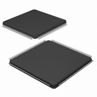
CY7C056V-12AXC Cypress Semiconductor Corp, CY7C056V-12AXC Datasheet - Page 13

CY7C056V-12AXC
Manufacturer Part Number
CY7C056V-12AXC
Description
IC SRAM 576KBIT 12NS 144LQFP
Manufacturer
Cypress Semiconductor Corp
Specifications of CY7C056V-12AXC
Format - Memory
RAM
Memory Type
SRAM - Dual Port, Asynchronous
Memory Size
576K (16K x 36)
Speed
12ns
Interface
Parallel
Voltage - Supply
3 V ~ 3.6 V
Operating Temperature
0°C ~ 70°C
Package / Case
144-LQFP
Density
576Kb
Access Time (max)
12ns
Sync/async
Asynchronous
Architecture
Not Required
Clock Freq (max)
Not RequiredMHz
Operating Supply Voltage (typ)
3.3V
Address Bus
14b
Package Type
TQFP
Operating Temp Range
0C to 70C
Number Of Ports
2
Supply Current
385mA
Operating Supply Voltage (min)
3.135V
Operating Supply Voltage (max)
3.465V
Operating Temperature Classification
Commercial
Mounting
Surface Mount
Pin Count
144
Word Size
36b
Number Of Words
16K
Lead Free Status / RoHS Status
Lead free / RoHS Compliant
Available stocks
Company
Part Number
Manufacturer
Quantity
Price
Company:
Part Number:
CY7C056V-12AXC
Manufacturer:
CY
Quantity:
8
Company:
Part Number:
CY7C056V-12AXC
Manufacturer:
ON
Quantity:
6 393
Company:
Part Number:
CY7C056V-12AXC
Manufacturer:
Cypress Semiconductor Corp
Quantity:
10 000
Switching Waveforms
Document #: 38-06055 Rev. *E
Notes
CE
30. R/W must be HIGH during all address transitions.
31. A write occurs during the overlap (t
32. t
33. If OE is LOW during a R/W controlled write cycle, the write pulse width must be the larger of t
34. To access RAM, CE
35. To access byte B
36. Transition is measured ±150 mV from steady state with a 5-pF load (including scope and jig). This parameter is sampled and not 100% tested.
37. During this period, the I/O pins are in the output state, and input signals must not be applied.
38. If the CE
DATA OUT
ADDRESS
ADDRESS
CE
DATA IN
DATA IN
0
to be placed on the bus for the required t
as short as the specified t
To access byte B
To access byte B
To access byte B
state.
, CE
0
HA
, CE
is measured from the earlier of CE
R/W
R/W
OE
1
[34, 35]
1
[34, 35]
0
LOW and CE
0
1
2
3
, CE
, CE
, CE
, CE
0
= V
0
0
0
0
1
= V
= V
= V
= V
HIGH or SEM LOW transition occurs simultaneously with or after the R/W LOW transition, the outputs remain in the high-impedance
IL
PWE
, CE
IL
IL
IL
IL
, B
, B
, B
, B
.
t
t
1
SA
SA
0
1
2
3
=SEM = V
NOTE 37
= V
= V
= V
= V
(continued)
SCE
IL
IL
IL
IL
0
, CE
, CE
, CE
, CE
Write Cycle No. 1: R/W Controlled Timing
or t
/CE
SD
Write Cycle No. 2: CE Controlled Timing
IH
PWE
1
. If OE is HIGH during an R/W controlled write cycle, this requirement does not apply and the write pulse can be
1
1
1
1
=SEM = V
=SEM = V
=SEM = V
=SEM = V
.
or R/W or (SEM or R/W) going HIGH at the end of Write Cycle.
) of CE
t
HZWE
0
IH
IH
IH
IH
=V
[36]
.
.
.
.
IL
CHIP SELECT VALID
t
t
and CE
AW
CHIP SELECT VALID
AW
t
t
WC
WC
1
t
t
SCE
=V
PWE
IH
[33]
or SEM=V
t
t
IL
SD
SD
and B
PWE
0–3
LOW.
or (t
HZWE
t
t
HA
HA
[30, 31, 32, 38]
[30, 31, 32, 33]
t
t
+ t
HD
HD
t
SD
LZWE
) to allow the I/O drivers to turn off and data
t
HZOE
NOTE 37
[36]
CY7C056V
CY7C057V
Page 13 of 26
[+] Feedback


