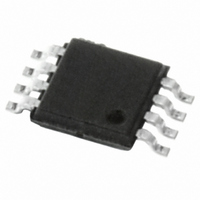
M25P05-AVDW6TP NUMONYX, M25P05-AVDW6TP Datasheet - Page 16

M25P05-AVDW6TP
Manufacturer Part Number
M25P05-AVDW6TP
Description
IC FLASH 512KBIT 50MHZ 8TSSOP
Manufacturer
NUMONYX
Series
Forté™r
Datasheet
1.M25P05-AVMN6T.pdf
(42 pages)
Specifications of M25P05-AVDW6TP
Format - Memory
FLASH
Memory Type
FLASH
Memory Size
512K (64K x 8)
Speed
50MHz
Interface
SPI, 3-Wire Serial
Voltage - Supply
2.7 V ~ 3.6 V
Operating Temperature
-40°C ~ 85°C
Package / Case
8-TSSOP
Lead Free Status / RoHS Status
Lead free / RoHS Compliant
Available stocks
Company
Part Number
Manufacturer
Quantity
Price
M25P05-A
Write Status Register (WRSR)
The Write Status Register (WRSR) instruction al-
lows new values to be written to the Status Regis-
ter. Before it can be accepted, a Write Enable
(WREN) instruction must previously have been ex-
ecuted. After the Write Enable (WREN) instruction
has been decoded and executed, the device sets
the Write Enable Latch (WEL).
The Write Status Register (WRSR) instruction is
entered by driving Chip Select (S) Low, followed
by the instruction code and the data byte on Serial
Data Input (D).
The instruction sequence is shown in
The Write Status Register (WRSR) instruction has
no effect on b6, b5, b4, b1 and b0 of the Status
Register. b6, b5 and b4 are always read as 0.
Chip Select (S) must be driven High after the
eighth bit of the data byte has been latched in. If
not, the Write Status Register (WRSR) instruction
is not executed. As soon as Chip Select (S) is driv-
en High, the self-timed Write Status Register cycle
(whose duration is t
Status Register cycle is in progress, the Status
Register may still be read to check the value of the
Write In Progress (WIP) bit. The Write In Progress
(WIP) bit is 1 during the self-timed Write Status
Register cycle, and is 0 when it is completed. At
some unspecified time before the cycle is complet-
ed, the Write Enable Latch (WEL) is reset.
The Write Status Register (WRSR) instruction al-
lows the user to change the values of the Block
Protect (BP1, BP0) bits, to define the size of the
area that is to be treated as read-only, as defined
in
struction also allows the user to set or reset the
Status Register Write Disable (SRWD) bit in ac-
cordance with the Write Protect (W) signal. The
Status Register Write Disable (SRWD) bit and
Write Protect (W) signal allow the device to be put
in the Hardware Protected Mode (HPM). The Write
Status Register (WRSR) instruction is not execut-
ed once the Hardware Protected Mode (HPM) is
entered.
16/42
Table 2.
The Write Status Register (WRSR) in-
W
) is initiated. While the Write
Figure 12.
The protection features of the device are summa-
rized in
When the Status Register Write Disable (SRWD)
bit of the Status Register is 0 (its initial delivery
state), it is possible to write to the Status Register
provided that the Write Enable Latch (WEL) bit has
previously been set by a Write Enable (WREN) in-
struction, regardless of the whether Write Protect
(W) is driven High or Low.
When the Status Register Write Disable (SRWD)
bit of the Status Register is set to 1, two cases
need to be considered, depending on the state of
Write Protect (W):
– If Write Protect (W) is driven High, it is possible
– If Write Protect (W) is driven Low, it is not pos-
Regardless of the order of the two events, the
Hardware Protected Mode (HPM) can be entered:
– by setting the Status Register Write Disable
– or by driving Write Protect (W) Low after setting
The only way to exit the Hardware Protected Mode
(HPM) once entered is to pull Write Protect (W)
High.
If Write Protect (W) is permanently tied High, the
Hardware Protected Mode (HPM) can never be
activated, and only the Software Protected Mode
(SPM), using the Block Protect (BP1, BP0) bits of
the Status Register, can be used.
to write to the Status Register provided that the
Write Enable Latch (WEL) bit has previously
been set by a Write Enable (WREN) instruction.
sible to write to the Status Register even if the
Write Enable Latch (WEL) bit has previously
been set by a Write Enable (WREN) instruction.
(Attempts to write to the Status Register are re-
jected, and are not accepted for execution). As
a consequence, all the data bytes in the memo-
ry area that are software protected (SPM) by the
Block Protect (BP1, BP0) bits of the Status Reg-
ister, are also hardware protected against data
modification.
(SRWD) bit after driving Write Protect (W) Low
the Status Register Write Disable (SRWD) bit.
Table 7.


