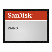
SDIN2C2-2G-T SanDisk, SDIN2C2-2G-T Datasheet - Page 22

SDIN2C2-2G-T
Manufacturer Part Number
SDIN2C2-2G-T
Description
IC INAND FLASH 2GB 169FBGA
Manufacturer
SanDisk
Type
Flash Diskr
Specifications of SDIN2C2-2G-T
Format - Memory
FLASH
Memory Type
FLASH - Nand
Memory Size
16G (2G x 8)
Speed
50MHz
Interface
SD/SPI Serial
Voltage - Supply
2.7 V ~ 3.6 V
Operating Temperature
-25°C ~ 85°C
Package / Case
169-FBGA
Density
2GByte
Operating Supply Voltage (typ)
3.3V
Operating Temperature (min)
-25C
Operating Temperature (max)
85C
Package Type
TFBGA
Mounting
Surface Mount
Pin Count
169
Operating Temperature Classification
Commercial
Operating Supply Voltage (min)
2.7V
Operating Supply Voltage (max)
3.6V
Programmable
Yes
Lead Free Status / RoHS Status
Lead free / RoHS Compliant
Available stocks
Company
Part Number
Manufacturer
Quantity
Price
Rev. 1.2
4.
4.1. General Description
iNAND protocol information is contained in this chapter; information includes bus protocol, card identification, and
a functional description.
4.2. SD Bus Protocol
Communication over the SD bus is based on command and data-bit streams initiated by a start bit and terminated by
a stop bit. See Section 3.6.1 of the SDA Physical Layer Specification, Version 2.00 for details.
4.3. Functional Description
The host controls all communication between itself and iNAND. To demonstrate how this communication works,
this section provides a general overview of the identification and data transfer modes; commands; dependencies;
various operation modes and restrictions for controlling the clock signal. All iNAND commands, together with
corresponding responses, state transitions, error conditions, and timings are also provided. For detailed information,
refer to Section 4 of the SDA Physical Layer Specification, Version 2.00.
4.3.1. Identification Mode
In Card Identification Mode the host resets all SD devices, validates operation voltage range, identifies and requests
to publish a relative address. For more information see Section 4.2 in the SDA Physical Layer Specification, Version
2.00.
4.3.2. Data Transfer Mode
In Data Transfer Mode, the host may operate iNAND in the f
about data read and write, erase, write protect management, lock/unlock operations, application-specific commands,
the switch function command, high-speed mode, the command system, the Send Interface Condition command
(CMD8). CMD8 is part of identification mode and command functional differences in high capacity iNAND. For
more detailed information, refer to Section 4.3 of the SDA Physical Layer Specification, Version 2.00.
4.3.3. Clock Control
The host can use the bus clock signal in iNAND to switch them to energy saving mode or to control data flow on the
bus. See Section 4.4 of the SDA Physical Layer Specification, Version 2.00.
4.3.4. Cyclic Redundancy Codes
The Cyclic Redundancy Check (CRC) protects against transmission errors that may occur on the iNAND bus.
Detailed information and examples for CRC7 and CRC16 are provided in Section 4.5 of the SDA Physical Layer
Specification, Version 2.00.
4.3.5. Error Conditions
See Section 4.6 of the SDA Physical Layer Specification, Version 2.00.
4.3.6. Commands
See Section 4.7 of the SDA Physical Layer Specification, Version 2.00 for detailed information about iNAND
commands.
© 2007 SanDisk Corporation
I
NAND P
ROTOCOL
D
ESCRIPTION
22
PP
frequency range. This section contains information
iNAND Protocol Description
SanDisk iNAND Data Sheet
80-36-00592


