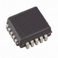
AT17C002-10JI Atmel, AT17C002-10JI Datasheet - Page 5

AT17C002-10JI
Manufacturer Part Number
AT17C002-10JI
Description
IC SRL CONFIG EEPROM 2M 20PLCC
Manufacturer
Atmel
Datasheet
1.AT17C002-10CI.pdf
(19 pages)
Specifications of AT17C002-10JI
Programmable Type
Serial EEPROM
Memory Size
2Mb
Voltage - Supply
4.5 V ~ 5.5 V
Operating Temperature
-40°C ~ 85°C
Package / Case
20-LCC (J-Lead)
Lead Free Status / RoHS Status
Contains lead / RoHS non-compliant
FPGA Master Serial
Mode Summary
Control of
Configuration
Cascading Serial
Configuration
EEPROMs
AT17 Series Reset
Polarity
Programming Mode
Standby Mode
2281D–12/01
The I/O and logic functions of any SRAM-based FPGA are established by a configura-
tion program. The program is loaded either automatically upon power-up, or on
command, depending on the state of the FPGA mode pins. In Master Mode, the FPGA
automatically loads the configuration program from an external memory. The AT17
Serial Configuration EEPROM has been designed for compatibility with the Master
Serial Mode.
This document discusses the AT40K, AT40KAL and AT94KAL applications, as well as
Xilinx applications.
Most connections between the FPGA device and the AT17 Serial EEPROM are simple
and self-explanatory:
•
•
•
•
•
For multiple FPGAs configured as a daisy-chain, or for FPGAs requiring larger configu-
ration memories, cascaded Configurators provide additional memory.
As the last bit from the first Configurator is read, the clock signal to the Configurator
asserts its CEO output Low and disables its DATA line driver. The second Configurator
recognizes the Low level on its CE input and enables its DATA output.
After configuration is complete, the address counters of all cascaded Configurators are
reset if the RESET/OE on each Configurator is driven to its active (Low) level.
If the address counters are not to be reset upon completion, then the RESET/OE input
can be tied to its inactive (High) level.
The AT17 Series Configurator allows the user to program the reset polarity as either
RESET/OE or RESET/OE. This feature is supported by industry-standard programmer
algorithms.
The programming mode is entered by bringing SER_EN Low. In this mode the chip can
be programmed by the 2-wire serial bus. The programming is done at V
Programming super voltages are generated inside the chip. The AT17C parts are
read/write at 5V nominal. The AT17LV parts are read/write at 3.3V nominal.
The AT17C/LV002 Series Configurator enters a low-power standby mode whenever CE
is asserted High. In this mode, the Configurator consumes less than 0.5 mA of current at
5V. The output remains in a high-impedance state regardless of the state of the OE
input.
The DATA output of the AT17 Series Configurator drives DIN of the FPGA devices.
The master FPGA CCLK output drives the CLK input of the AT17 Series
Configurator.
The CEO output of any AT17 Series Configurator drives the CE input of the next
Configurator in a cascade chain of EEPROMs.
SER_EN must be connected to V
The READY pin is available as an open-collector indicator of the device’s reset
status; it is driven Low while the device is in its power-on reset cycle and released
(tri-stated) when the cycle is complete.
CC
(except during ISP).
AT17C/LV002
CC
supply only.
5


