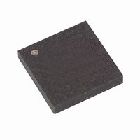
AT17C512-10CI Atmel, AT17C512-10CI Datasheet

AT17C512-10CI
Specifications of AT17C512-10CI
Related parts for AT17C512-10CI
AT17C512-10CI Summary of contents
Page 1
... Low-power Standby Mode Description The AT17C512/010 and AT17LV512/010 (high-density AT17 Series) FPGA Configuration EEPROMs (Configurators) provide an easy-to-use, cost-effective con- figuration memory for Field Programmable Gate Arrays. The AT17 Series is packaged in the popular 20-pin PLCC. The AT17 Series family uses a simple serial-access pro- cedure to configure one or more FPGA devices ...
Page 2
... Controlling the High- density AT17 Series Serial EEPROMs During Configuration AT17C512/010/LV512/010 2 The I/O and logic functions of the FPGA and their associated interconnections are established by a configuration program. The program is loaded either automatically upon power-up command, depending on the state of the FPGA mode pins. In Master Mode, the FPGA automatically loads the configuration program from an external memory ...
Page 3
... Low) level. The AT17 Series Configurator allows the user to program the reset polarity as either RESET/OE or RESET/OE. This feature is supported by industry-standard programmer algorithms. For more details on programming the EEPROMs reset polarity, please AT17C512/010/LV512/010 AT17C512/010 AT17LV512/010 DATA CLK CE ...
Page 4
... GND AT17C512/010/LV512/010 4 reference the “Programming Specification for Atmel’s FPGA Configuration EEPROMs” application note. The programming mode is entered by bringing SER_EN Low. In this mode the chip can be programmed by the 2-wire serial bus. The programming is done at VCC supply only. Programming super voltages are generated inside the chip. See the “Programming Specification for Atmel’ ...
Page 5
... Open collector reset state indicator. Driven Low during power-up reset, released when power-up is complete. (Recommend a 4.7 kΩ pull-up on this pin if used). The DIP/SOIC package. I Serial enable must be held High during FPGA loading operations. Bringing SER_EN Low enables the 2-wire Serial Programming Mode. +3.3V/+5V power supply pin. AT17C512/010/LV512/010 5 ...
Page 6
... Supply voltage relative to GND V CC -40°C to +85°C Military Supply voltage relative to GND -55°C to +125°C AT17C512/010/LV512/010 6 *NOTICE: Stresses beyond those listed under Absolute Maximum Ratings may cause permanent dam- age to the device. These are stress ratings only, and functional operation of the device at these or any other conditions beyond those listed under +0 ...
Page 7
... OL V High-level Output Voltage ( Low-level Output Voltage ( High-level Output Voltage ( Low-level Output Voltage ( Supply Current, Active Mode CCA I Input or Output Leakage Current ( Supply Current, Standby Mode CCS AT17C512/010/LV512/010 = -4 mA) OH Commercial = +4 mA mA) OH Industrial = +4 mA mA) OH Military = +4 mA GND Commercial Industrial/Military = -2.5 mA) ...
Page 8
... AC Characteristics Characteristics When Cascading RESET/OE CE CLK T CDF LAST BIT DATA T OCK CEO AT17C512/010/LV512/010 8 T SCE CAC T OCE T SCE T T HOE FIRST BIT T OOE T OCE HCE ...
Page 9
... MAX Input Clock Frequency MAX Notes: 1. Preliminary specifications for military operating range only test load = 50 pF. 3. Float delays are measured with loads. Transition is measured ±200 mV from steady state active levels. AC Characteristics for AT17C512/010 When Cascading V = 5V± 5% Commercial ± 10% Industrial/Military CC CC ...
Page 10
... RESET/OE to CEO Delay OOE F MAX Input Clock Frequency MAX Notes: 1. Preliminary specifications for military operating range only test load = 50 pF. 3. Float delays are measured with loads. Transition is measured ±200 mV from steady state active levels. AT17C512/010/LV512/010 10 Commercial Industrial/Military Min Max Min 50.0 55.0 55 ...
Page 11
... Ordering Information – 5V Devices Memory Size Ordering Code 512K AT17C512-10JC AT17C512-10PC AT17C512-10CC AT17C512-10JI AT17C512-10PI AT17C512-10CI 1M AT17C010-10JC AT17C010-10PC AT17C010-10CC AT17C010-10JI AT17C010-10PI AT17C010-10CI Ordering Information – 3.3V Devices Memory Size Ordering Code 512K AT17LV512-10JC AT17LV512-10PC AT17LV512-10CC AT17LV512-10JI AT17LV512-10PI AT17LV512-10CI 1M AT17LV010-10JC AT17LV010-10PC AT17LV010-10CC AT17LV010-10JI ...
Page 12
... JEDEC STANDARD MS-018 AA 0. 1.04 0. 1.14 REF 0.34 0.4 3 SIDE VIEW 4 AT17C512/010/LV512/010 .400 (10.16) .355 (9.02) PIN 1 .280 (7.11) .240 (6.10) .037 (.940) .027 (.690) .300 (7.62) REF .210 (5.33) MAX .100 (2.54) BSC SEATING PLANE .015 (.380) MIN .150 (3.81) ...
Page 13
... No licenses to patents or other intellectual property of Atmel are granted by the Company in connection with the sale of Atmel products, expressly or by implication. Atmel’s products are not authorized for use as critical components in life support devices or systems. ...


