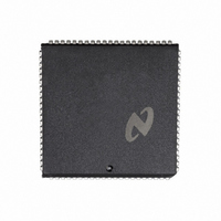
DP8422AV-25 National Semiconductor, DP8422AV-25 Datasheet - Page 3

DP8422AV-25
Manufacturer Part Number
DP8422AV-25
Description
IC CTRLR/DVR CMOS PROGRAM 84PLCC
Manufacturer
National Semiconductor
Datasheet
1.DP8420AV-25.pdf
(58 pages)
Specifications of DP8422AV-25
Controller Type
Dynamic RAM (DRAM)
Voltage - Supply
4.5 V ~ 5.5 V
Operating Temperature
0°C ~ 70°C
Package / Case
84-PLCC
Lead Free Status / RoHS Status
Contains lead / RoHS non-compliant
Other names
*DP8422AV-25
Available stocks
Company
Part Number
Manufacturer
Quantity
Price
Company:
Part Number:
DP8422AV-25
Manufacturer:
NDK
Quantity:
3
Company:
Part Number:
DP8422AV-25
Manufacturer:
Texas Instruments
Quantity:
10 000
Part Number:
DP8422AV-25
Manufacturer:
NS/国半
Quantity:
20 000
1 0 Introduction
The DP8420A 21A 22A are CMOS Dynamic RAM control-
lers that incorporate many advanced features which include
address latches refresh counter refresh clock row column
and refresh address multiplexer delay line refresh access
arbitration logic and high capacitive drivers The program-
mable system interface allows any manufacturer’s micro-
processor
DP8420A 21A 22A to DRAM arrays up to 64 Mbytes in
size
After power up the user must first reset and program the
DP8420A 21A 22A before accessing the DRAM The chip
is programmed through the address bus
Reset
Due to the differences in power supplies the internal reset
circuit may not always reset correctly therefore an External
(hardware) Reset must be performed before programming
the chip
Programming
After resetting the chip the user can program the controller
by either one of two methods Mode Load Only Program-
ming or Chip Select Access Programming
Initialization Period
Once the DP8420A 21A 22A has been programmed for the
first time a 60 ms initialization period is entered During this
time the DRC performs refreshes to the DRAM array so
further warm up cycles are unnecessary The initialization
period is entered only after the first programming after a
reset
Accessing Modes
After
DP8420A 21A 22A is ready to access the DRAM There
are two modes of accessing with these controllers Mode 0
which indicates RAS synchronously and Mode 1 which indi-
cates RAS asynchronously
Refresh Modes
The DP8420A 21A 22A have expanded refresh capabilities
compared to previous DRAM controllers There are three
modes of refreshing available Internal Automatic Refresh-
ing Externally Controlled Burst Refreshing and Refresh Re-
quest Acknowledge Refreshing Any of these modes can
be used together or separately to achieve the desired re-
sults
Refresh Types
These controllers have three types of refreshing available
Conventional Staggered and Error Scrubbing Any refresh
control mode can be used with any type of refresh
Wait Support
The DP8420A 21A 22A have wait support available as
DTACK or WAIT Both are programmable DTACK Data
Transfer ACKnowledge is useful for processors whose wait
signal is active high WAIT is useful for those processors
whose wait signal is active low The user can choose either
at programming These signals are used by the on chip arbi-
ter to insert wait states to guarantee the arbitration between
accesses refreshes and precharge Both signals are inde-
pendent of the access mode chosen and both signals can
be dynamically delayed further through the WAITIN signal to
the DP8420A 21A 22A
resetting
or
bus
and
to
programming
directly
interface
the
chip
via
the
the
3
Sequential Accesses (Static Column Page Mode)
The DP8420A 21A 22A have address latches used to
latch the bank row and column address inputs Once the
address is latched a COLumn INCrement (COLINC) feature
can be used to increment the column address The address
latches can also be programmed to be fall through COLINC
can be used for Sequential Accesses of Static Column
DRAMs Also COLINC in conjunction with ECAS inputs can
be used for Sequential Accesses to Page Mode DRAMs
RAS and CAS Configuration (Byte Writing)
The RAS and CAS drivers can be configured to drive a one
two or four bank memory array up to 32 bits in width The
ECAS signals can then be used to select one of four CAS
drivers for Byte Writing with no extra logic
Memory Interleaving
When configuring the DP820A 21A 22A for more than one
bank Memory Interleaving can be used By tying the low
order address bits to the bank select lines B0 and B1 se-
quential back to back accesses will not be delayed since
these controllers have separate precharge counters per
bank
Address Pipelining
The DP8420A 21A 22A are capable of performing Address
Pipelining In address pipelining the DRC will guarantee the
column address hold time and switch the internal multiple-
xor to place the row address on the address bus At this
time another memory access to another bank can be initiat-
ed
Dual Accessing
Finally the DP8422A has all the features previously men-
tioned and unlike the DP8420A 21A the DP8422A has a
second port to allow a second CPU to access the same
memory array The DP8422A has four signals to support
Dual Accessing these signals are AREQB ATACKB LOCK
and GRANTB All arbitration for the two ports and refresh is
done on chip by the controller through the insertion of wait
states Since the DP8422A has only one input address bus
the address lines must be multiplexed externally The signal
GRANTB can be used for this purpose
Terminology
The following explains the terminology used in this data
sheet The terms negated and asserted are used Asserted
refers to a ‘‘true’’ signal Thus ‘‘ECAS0 asserted’’ means
the ECAS0 input is at a logic 0 The term ‘‘COLINC assert-
ed’’ means the COLINC input is at a logic 1 The term negat-
ed refers to a ‘‘false’’ signal Thus ‘‘ECAS0 negated’’
means the ECAS0 input is at a logic 1 The term ‘‘COLINC
negated’’ means the input COLINC is at a logic 0 The table
shown below clarifies this terminology
Active High
Active High
Active Low
Active Low
Signal
Asserted
Asserted
Negated
Negated
Action
Logic Level
High
High
Low
Low


