LNK363PG Power Integrations, LNK363PG Datasheet - Page 8
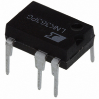
LNK363PG
Manufacturer Part Number
LNK363PG
Description
IC OFFLINE SWIT HV 8DIP
Manufacturer
Power Integrations
Series
LinkSwitch®-XTr
Type
Off Line Switcherr
Datasheet
1.LNK362PG.pdf
(16 pages)
Specifications of LNK363PG
Output Isolation
Isolated
Frequency Range
124 ~ 140kHz
Voltage - Output
700V
Power (watts)
7.5W
Operating Temperature
-40°C ~ 150°C
Package / Case
8-DIP (0.300", 7.62mm), 7 Leads
For Use With
596-1105 - DESIGN ACCELERATOR KIT XT SWITCH
Lead Free Status / RoHS Status
Lead free / RoHS Compliant
Other names
596-1242-5
Available stocks
Company
Part Number
Manufacturer
Quantity
Price

Part Number:
LNK363PG
Manufacturer:
POWER
Quantity:
20 000


Rev. E 11/08
DRAIN Voltage .................................. .............-0.3 V to 700 V
Peak DRAIN Current: LNK362................200 mA (375 mA)
FEEDBACK Voltage ........................................... -0.3 V to 9 V
FEEDBACK Current ...................................................100 mA
BYPASS Voltage.................................................. -0.3 V to 9 V
Storage Temperature .....................................-65 °C to 150 °C
Operating Junction Temperature
Lead Temperature
Thermal Impedance: P or G Package:
Output Frequency
Maximum Duty
Cycle
FEEDBACK Pin
Turnoff Threshold
Current
FEEDBACK Pin
Voltage at Turnoff
Threshold
DRAIN Supply
Current
BYPASS Pin
Charge Current
BYPASS Pin
Voltage
BYPASS Pin
Voltage Hysteresis
2-8
CONTROL FUNCTIONS
8
8
Parameter
LNK362-364
(θ
(θ
(θ
(θ
(4)
JA
JC
JA
JC
....................................................... 260 °C
) ........................... 70 °C/W
)
) ..................... .... 100 °C/W
)
(1)
D Package:
(2)
LNK363/364.........400 mA (750 mA)
............................................... 11 °C/W
............................................... 30 °C/W
Symbol
DC
V
f
V
I
I
V
OSC
I
I
I
CH1
CH2
(3)
FB
S1
S2
BPH
FB
BP
MAX
................-40 °C to 150 °C
ABSOLUTE MAXIMUM RATINGS
T
SOURCE = 0 V; T
J
T
= 25 °C
(Unless Otherwise Specifi ed)
J
125 °C
THERMAL IMPEDANCE
= 0 °C to
(MOSFET Not Switching)
(3)
(3)
V
V
; 60 °C/W
; 80 °C/W
FEEDBACK Open
BP
BP
Conditions
See Figure 8
= 0 V, T
= 4 V, T
See Note C
See Note C
See Note A
Switching)
T
(MOSFET
S2 Open
V
J
FB
= 25 °C
Peak-Peak Jitter
(2)
(2)
(4)
(4)
≥2 V
J
J
J
= -40 to 125 °C
= 25 °C
= 25 °C
Notes:
1. All voltages referenced to SOURCE, T
2. The higher peak DRAIN current is allowed while the
3. Normally limited by internal circuitry.
4. 1/16 in. from case for 5 seconds.
5. Maximum ratings specifi ed may be applied, one at a time,
Average
Notes:
1. Measured on pin 2 (SOURCE) close to plastic interface.
2. Measured on pin 8 (SOURCE) close to plastic interface.
3. Soldered to 0.36 sq. in. (232 mm
4. Soldered to 1 sq. in. (645 mm
LNK363-364
without causing permanent damage to the product.
Exposure to Absolute Maximum Rating conditions for
extended periods of time may affect product reliability.
DRAIN voltage is simultaneously less than 400 V.
LNK362
(1,5)
Min
1.55
1.53
5.55
-5.5
-3.8
124
0.8
60
30
2
), 2 oz. (610 g/m
Typ
1.65
1.63
-3.5
-2.3
132
200
250
2
5.8
1.0
49
), 2 oz. (610 g/m
9
A
Max
= 25 °C.
1.75
1.73
6.10
140
250
300
-1.8
-1.0
1.2
68
2
2
) copper clad.
) copper clad.
Units
kHz
mA
μA
μA
μA
%
V
V
V
Related parts for LNK363PG
Image
Part Number
Description
Manufacturer
Datasheet
Request
R

Part Number:
Description:
SOP-16
Manufacturer:
Power Integrations
Datasheet:
Part Number:
Description:
DIP8
Manufacturer:
Power Integrations
Datasheet:
Part Number:
Description:
TO-263
Manufacturer:
Power Integrations
Datasheet:
Part Number:
Description:
TO-263
Manufacturer:
Power Integrations
Datasheet:
Part Number:
Description:
Manufacturer:
Power Integrations
Datasheet: