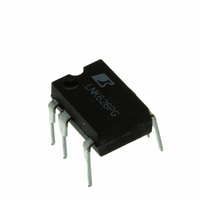
LNK623DG Power Integrations, LNK623DG Datasheet - Page 2

LNK623DG
Manufacturer Part Number
LNK623DG
Description
IC OFFLINE SWIT OTP OCP CV 8SOP
Manufacturer
Power Integrations
Series
LinkSwitch®-CVr
Datasheet
1.LNK625DG.pdf
(18 pages)
Specifications of LNK623DG
Output Isolation
Isolated
Frequency Range
93 ~ 106kHz
Voltage - Output
700V
Power (watts)
9W
Operating Temperature
-40°C ~ 150°C
Package / Case
8-SOIC (0.154", 3.90mm Width) 7 leads
Duty Cycle (max)
54 %
Operating Temperature Range
- 40 C to + 150 C
Mounting Style
SMD/SMT
Maximum Operating Temperature
+ 150 C
Minimum Operating Temperature
- 40 C
Number Of Outputs
3
Output Power
6 W
Lead Free Status / RoHS Status
Lead free / RoHS Compliant
Other names
596-1249-5
Available stocks
Company
Part Number
Manufacturer
Quantity
Price
Company:
Part Number:
LNK623DG
Manufacturer:
PowerInt
Quantity:
200
Company:
Part Number:
LNK623DG
Manufacturer:
POWER
Quantity:
15 000
Part Number:
LNK623DG
Manufacturer:
POWER
Quantity:
20 000
Company:
Part Number:
LNK623DG-TL
Manufacturer:
MICROCHIP
Quantity:
2 100
Part Number:
LNK623DG-TL
Manufacturer:
POWER
Quantity:
20 000
Rev. E 09/09
Figure 2
Pin Functional Description
DRAIN (D) Pin:
This pin is the power MOSFET drain connection. It provides
internal operating current for both start-up and steady-state
operation.
BYPASS (BP) Pin:
This pin is the connection point for an external bypass capacitor
for the internally generated 6 V supply.
FEEDBACK (FB) Pin:
During normal operation, switching of the power MOSFET is
controlled by this pin. This pin senses the AC voltage on the
bias winding. This control input regulates the output voltage
based on the fl yback voltage of the bias winding.
SOURCE (S) Pin:
This pin is internally connected to the output MOSFET source
for high voltage power and control circuit common returns.
2
FEEDBACK
SOURCE
BYPASS
Functional Block Diagram.
(BP)
(FB)
(S)
LNK623-626
6.5 V
V
TH
+
FB
-
t
SAMPLE-OUT
DC
MAX
I
LIM
OSCILLATOR
Auto-Restart
Open-Loop
FAULT
D
Q
OUT
FB
I
LIM
DC
MACHINE
MAX
STATE
Drive
Reset
Figure 3.
V
SHUTDOWN
ILIMIT
BP
THERMAL
FB
P Package (DIP-8C)
D
Current Limit
Comparator
t
1
2
4
Pin Confi guration.
SAMPLE-OUT
6 V
5 V
+
-
3a
V
+
-
ILIMIT
SAMPLE
BLANKING
DELAY
LEADING
8
7
6
5
EDGE
S
S
S
S
REGULATOR
6 V
D Package (SO-8C)
FB
BP
D
1
2
4
www.powerint.com
3b
SOURCE
DRAIN
PI-5198-071608
(D)
(S)
8
PI-5197-110408
7
6
5
S
S
S
S


