TOP258PN Power Integrations, TOP258PN Datasheet
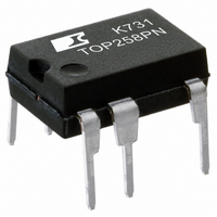
TOP258PN
Specifications of TOP258PN
Available stocks


Related parts for TOP258PN

TOP258PN Summary of contents
Page 1
... W TOP254MN TOP255PN/ TOP255MN TOP256PN/ TOP256MN TOP257PN/ TOP257MN TOP258PN/ TOP258MN Table 1. Output Power Table. (for notes see page 2). www.powerint.com AC IN Figure 1. Heatsink is connected to SOURCE for low EMI • Improved auto-restart delivers <3% of maximum power in • short circuit and open loop fault conditions Accurate hysteretic thermal shutdown function automatically • ...
Page 2
TOP252-262 ® EcoSmart – Energy Effi cient Energy effi cient over entire load range • No-load consumption • Less than 200 mW at 230 VAC • Standby power for 1 W input • >600 mW output at 110 VAC input ...
Page 3
Functional Block Diagram ....................................................................................................................................... 4 Pin Functional Description ...................................................................................................................................... 6 TOPSwitch-HX Family Functional Description ....................................................................................................... 7 CONTROL (C) Pin Operation .................................................................................................................................... 8 Oscillator and Switching Frequency .......................................................................................................................... 8 Pulse Width Modulator ............................................................................................................................................ 9 Maximum Load Cycle .............................................................................................................................................. 9 Error Amplifi ...
Page 4
TOP252-262 V C CONTROL ( SHUNT REGULATOR/ ERROR AMPLIFIER - 5 (LIMIT) CURRENT LIMIT ADJUST ON/OFF STOP LOGIC MULTI- FUNCTION (M) V OVP OV/ UV LINE DC ...
Page 5
V C CONTROL ( SHUNT REGULATOR/ ERROR AMPLIFIER - + 5 (LIMIT) CURRENT LIMIT ADJUST ON/OFF EXTERNAL CURRENT LIMIT (X) STOP LOGIC VOLTAGE MONITOR ( ...
Page 6
TOP252-262 Pin Functional Description DRAIN (D) Pin: High-voltage power MOSFET DRAIN pin. The internal start-up bias current is drawn from this pin through a switched high- voltage current source. Internal current limit sense point for drain current. CONTROL (C) Pin: ...
Page 7
DC Input Voltage D M CONTROL Figure 8. P/G Package Externally Set Current Limit. reduction, output overvoltage protection (OVP), external current limit adjustment, remote ON/OFF and device reset. A connection to SOURCE pin disables all ...
Page 8
TOP252-262 4. Switching frequency of 132 kHz reduces the transformer size with no noticeable impact on EMI. 5. Frequency jittering reduces EMI in the full frequency mode at high load condition. 6. Hysteretic over-temperature shutdown ensures automatic recovery from thermal ...
Page 9
OSC Switching Frequency f - OSC DRAIN Figure 10. Switching Frequency Jitter (Idealized V (half frequency), which may be preferable in some cases such as noise sensitive video applications or a high effi ciency standby ...
Page 10
TOP252-262 LINE 0 V S14 S15 S13 S12 DRAIN OUT Note: S0 through S15 are the output states of the auto-restart counter Figure 11. Typical ...
Page 11
Line Overvoltage Shutdown (OV) The same resistor used for UV also sets an overvoltage threshold, which, once exceeded, will force TOPSwitch-HX to stop switching instantaneously (after completion of the current switching cycle). If this condition lasts for at least 100 ...
Page 12
TOP252-262 X Pin (Enabled) Output MOSFET Switching (Disabled) I (Default) LIMIT Current Limit DC (78%) MAX Maximum Duty Cycle V BG Pin Voltage -250 -200 -150 X and V Pins ( and M Packages) and M Pin (P ...
Page 13
Line Feed-Forward with DC Reduction MAX The same resistor used for UV and OV also implements line voltage feed-forward, which minimizes output line ripple and reduces power supply output sensitivity to line transients. Note that for the same CONTROL pin ...
Page 14
TOP252-262 CONTROL (C) EXTERNAL CURRENT LIMIT (X) VOLTAGE MONITOR (V) Figure 13a. VOLTAGE MONITOR (V) and EXTERNAL CURRENT LIMIT (X) Pin Input Simplifi ed Schematic. CONTROL (C) MULTI-FUNCTION (M) Figure 13b. MULTI-FUNCTION (M) Pin Input Simplifi ed Schematic. 14 Rev. ...
Page 15
Typical Uses of FREQUENCY (F) Pin + DC D Input CONTROL Voltage Figure 14. Full Frequency Operation (132 kHz). www.powerint.com Input Voltage C PI-2654-071700 Figure 15. Half Frequency Operation (66 kHz). TOP252-262 + DC D CONTROL C ...
Page 16
TOP252-262 Typical Uses of VOLTAGE MONITOR (V) and EXTERNAL CURRENT LIMIT (X) Pins TOP252-258M + Input D Voltage D V CONTROL Figure 16a. Three Terminal Operation (VOLTAGE MONITOR and EXTERNAL CURRENT LIMIT ...
Page 17
Typical Uses of VOLTAGE MONITOR (V) and EXTERNAL CURRENT LIMIT (X) Pins (cont Input Voltage D V CONTROL C 6 Figure 20. Line Sensing for Undervoltage Only (Overvoltage Disabled ...
Page 18
TOP252-262 Typical Uses of VOLTAGE MONITOR (V) and EXTERNAL CURRENT LIMIT (X) Pins (cont Input Voltage CONTROL TOP259-261YN would S X use the G pin as the return for ...
Page 19
Typical Uses of MULTI-FUNCTION (M) Pin (cont Input Voltage D M CONTROL S - Figure 31. Line Sensing for Undervoltage, Overvoltage, Line Feed-Forward and Latched Output Overvoltage Protection ...
Page 20
TOP252-262 Typical Uses of MULTI-FUNCTION (M) Pin (cont output or can be replaced by a manual switch. DC Input Voltage D M CONTROL Q R ON/OFF Figure 37. Active-on (Fail Safe) Remote ON/OFF. + ...
Page 21
... 265 VAC Figure 41 Dual Output Power Supply using TOP258PN. www.powerint.com winding. Zener VR2 will break down and current will fl ow into the “M” pin of the TOPSwitch initiating a hysteretic overvoltage protection with automatic restart attempts. Resistor R5 will limit the current into the M pin to < 336 μA, thus setting hysteretic OVP. If latching OVP is desired, the value of R5 can be reduced to 20 Ω ...
Page 22
TOP252-262 A High Effi ciency, 150 W, 250 – 380 VDC Input Power Supply The circuit shown in Figure 42 delivers 150 84% effi ciency using a TOP258Y from a 250 VDC to ...
Page 23
A High Effi ciency continuous – Peak, Universal Input Power Supply The circuit shown in Figure 43 takes advantage of several of TOPSwitch-HX features to reduce system cost and power supply size and to improve power ...
Page 24
TOP252-262 A High Effi ciency Universal Input Power Supply The circuit shown in Figure 44 delivers 88% effi ciency using a TOP260EN operating over an input voltage range of 90 ...
Page 25
Key Application Considerations TOPSwitch-HX vs. TOPSwitch-GX Table 4 compares the features and performance differences between TOPSwitch-HX and TOPSwitch-GX. Many of the new TOPSwitch-HX vs. TOPSwitch-GX Function TOPSwitch-GX EcoSmart Linear frequency reduction to 30 kHz (@ 132 kHz) for duty cycles ...
Page 26
TOP252-262 TOPSwitch-HX Design Considerations Power Table The data sheet power table (Table 1) represents the maximum practical continuous output power based on the following conditions output. 2. Schottky or high effi ciency output diode. 3. 135 V ...
Page 27
Frequency (MHz) Figure 45a. Fixed Frequency Operation Without Jitter TOPSwitch-HX (with jitter -10 0 -10 -20 0.15 1 Frequency (MHz) ...
Page 28
TOP252-262 Optional PCB slot for external heatsink in contact with SOURCE pins Input Filter Capacitor JP1 R1 Maximize hatched copper areas ( ) for optimum heat sinking Figure 46. Layout Considerations for TOPSwitch-HX Using P-Package. ...
Page 29
Input Filter Capacitor J1 HS1 + JP1 R1 R3 Figure 48. Layout Considerations for TOPSwitch-HX Using TOP254-258 Y-Package. Input Filter Capacitor JP1 R11 Figure 49. Layout Considerations for TOPSwitch-HX Using TOP259-261 Y-Package. ...
Page 30
TOP252-262 Input Filter Capacitor R11 R5 Figure 50a. Layout Considerations for TOPSwitch-HX Using E-Package and Operating at 66 kHz. Input Filter Capacitor ...
Page 31
... DRAIN pin and attached to the same heat sink, having a resistance value that is equal to the difference between the measured R the worst case maximum specifi cation. does not DS Design Tools Up-to-date information on design tools can be found at the Power Integrations website: www.powerint.com TOP252-262 R12 C16 D8 HS2 Output Rectifier ...
Page 32
TOP252-262 Absolute Maximum Ratings (2) DRAIN Peak Voltage .................................................................. -0 700 V DRAIN Peak Current: TOP252 ................................................................ 0.68 A DRAIN Peak Current: TOP253 ................................................................. 1.37 A DRAIN Peak Current: TOP254 ................................................................ 2.08 A DRAIN Peak Current: TOP255 .................................................................2.72 ...
Page 33
Parameter Symbol Control Functions (cont.) External Bias Current I B CONTROL Current Duty Cycle C(OFF) Dynamic Impedance Z C Dynamic Impedance Temperature Drift CONTROL Pin Internal Filter Pole Upper Peak Current to k Set Current Limit Ratio ...
Page 34
TOP252-262 Parameter Symbol Multi-Function (M), Voltage Monitor (V) and External Current Limit (X) Inputs Output Overvoltage Latching Shutdown I OV(LS) Threshold Current Pin Reset Voltage V(TH) V M(TH) Remote ON/OFF Negative Threshold I Current and ...
Page 35
... TOP257PN/GN di/dt = 155 mA/μ °C J TOP257MN di/dt = 265 mA/μ °C J TOP257LN di/dt = 530 mA/μ °C J TOP257YN/EN di/dt = 705 mA/μ °C J TOP258PN/GN di/dt = 170 mA/μ °C J TOP258MN di/dt = 310 mA/μ °C J TOP258LN di/dt = 620 mA/μ °C J TOP252-262 Min Typ Max Units 0.400 ...
Page 36
TOP252-262 Parameter Symbol Circuit Protection (cont.) Self Protection Current Limit I LIMIT (See Note C) Initial Current Limit I INIT Power Coeffi cient P COEFF Leading Edge t Blanking Time LEB Current Limit Delay t IL(D) Thermal Shutdown Temperature Thermal ...
Page 37
Parameter Symbol Output (cont.) ON-State R Resistance DS(ON) DRAIN Supply Voltage OFF-State Drain I Leakage Current DSS Breakdown BV Voltage DSS Rise Time t R Fall Time t F Supply Voltage Characteristics I CD1 Control Supply/ Discharge Current I CD2 ...
Page 38
TOP252-262 VOLTAGE Figure 51. Duty Cycle Measurement. 120 100 Dynamic Impedance CONTROL Pin Voltage (V) Figure 52. CONTROL Pin I-V Characteristic. TOP254-258 Y, all Packages (X and V ...
Page 39
Typical Performance Characteristics 1.1 1 0.9 0.8 0.7 0.6 0.5 0.4 0.3 Notes: 1. Maximum and Minimum levels are 0.2 based on characterization 125 0 -200 Figure 55a. Normalized Current Limit ...
Page 40
TOP252-262 Typical Performance Characteristics (cont.) 1.1 1.0 0.9 -50 - Junction Temperature ( C) Figure 56. Breakdown Voltage vs. Temperature. 1.2 1.0 0.8 0.6 0.4 0.2 0 -50 - Junction Temperature ( C) Figure ...
Page 41
Typical Performance Characteristics (cont.) 6 5.5 5 4.5 4 3 100 200 300 VOLTAGE-MONITOR Pin Current ( A) Figure 62a. VOLTAGE-MONITOR Pin vs. Current See expanded 1 version (Figure 63b) 0 ...
Page 42
TOP252-262 Typical Performance Characteristics (cont CASE T = 100 C CASE Drain Voltage (V) Figure 66. Output Characteristics. 10000 ...
Page 43
PIN 1 .050 (1.27) BSC .150 (3.81) BSC .050 (1.27) .050 (1.27) .050 (1.27) .200 (5.08) .100 (2.54) PIN 1 .150 (3.81) MOUNTING HOLE PATTERN Y07C www.powerint.com ...
Page 44
TOP252-262 ⊕ .004 (.10) -E- .240 (6.10) .260 (6.60) Pin 1 .367 (9.32) -D- .387 (9.83) .125 (3.18) .145 (3.68) -T- SEATING PLANE .100 (2.54) BSC .048 (1.22) .053 (1.35) .014 (.36) ⊕ .010 ...
Page 45
D S .004 (.10) -E- .240 (6.10) .260 (6.60) Pin 1 .100 (2.54) (BSC) .367 (9.32) -D- .387 (9.83) .125 (3.18) .145 (3.68) .032 (.81) .048 (1.22) .037 (.94) .053 (1.35) www.powerint.com SMD-8C .046 .060 .086 .186 .372 (9.45) ...
Page 46
TOP252-262 2 0.403 (10.24) A 0.397 (10.08 0.325 (8.25) 0.320 (8.13) Pin #1 I.D. 0.070 (1.78) Ref. 0.050 (1.27) 3 0.020 M 0. FRONT VIEW 10° Ref. All Around 0.021 (0.53) 0.019 (0.48) 0.048 (1.22) 0.046 ...
Page 47
A 0.397 (10.08) B 0.325 (8.25) 2 0.320 (8.13 Pin 1 I.D. 0.070 (1.78) Ref. 0.050 (1.27) BOTTOM VIEW Exposed pad hidden 1 7 0.060 (1.52) Ref. 0.019 (0.48) Ref. 0.378 (9.60) Ref. END VIEW ...
Page 48
... The products and applications illustrated herein (including transformer construction and circuits external to the products) may be covered by one or more U.S. and foreign patents, or potentially by pending U.S. and foreign patent applications assigned to Power Integrations. A complete list of Power Integrations patents may be found at www.powerint.com. Power Integrations grants its customers a license under certain patent rights as set forth at http://www ...