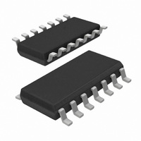
TEA1522T/N2,518 NXP Semiconductors, TEA1522T/N2,518 Datasheet - Page 16

TEA1522T/N2,518
Manufacturer Part Number
TEA1522T/N2,518
Description
IC CTRLR SMPS OCP UVD HV 14SOIC
Manufacturer
NXP Semiconductors
Series
STARplug™r
Specifications of TEA1522T/N2,518
Package / Case
14-SOIC (0.154", 3.90mm Width)
Output Isolation
Isolated
Frequency Range
10 ~ 200kHz
Voltage - Input
7.5 ~ 40 V
Voltage - Output
650V
Power (watts)
1W
Operating Temperature
-40°C ~ 145°C
Output Power
30 W
Input Voltage
2.5 V
Switching Frequency
550 KHz
Operating Temperature Range
- 20 C to + 85 C
Mounting Style
SMD/SMT
Duty Cycle (max)
75 %
Lead Free Status / RoHS Status
Lead free / RoHS Compliant
For Use With
568-4326 - KIT DEMO STARPLUG BRONCO II
Lead Free Status / Rohs Status
Lead free / RoHS Compliant
Other names
568-2438-2
935269967518
TEA1522T/N2
TEA1522TD-T
935269967518
TEA1522T/N2
TEA1522TD-T
Available stocks
Company
Part Number
Manufacturer
Quantity
Price
Company:
Part Number:
TEA1522T/N2,518
Manufacturer:
ALI
Quantity:
68
Philips Semiconductors
TEA152X_FAM_2
Product data sheet
16.3.2 Wave soldering
Several methods exist for reflowing; for example, convection or convection/infrared
heating in a conveyor type oven. Throughput times (preheating, soldering and cooling)
vary between 100 seconds and 200 seconds depending on heating method.
Typical reflow peak temperatures range from 215 C to 270 C depending on solder paste
material. The top-surface temperature of the packages should preferably be kept:
Moisture sensitivity precautions, as indicated on packing, must be respected at all times.
Conventional single wave soldering is not recommended for surface mount devices
(SMDs) or printed-circuit boards with a high component density, as solder bridging and
non-wetting can present major problems.
To overcome these problems the double-wave soldering method was specifically
developed.
If wave soldering is used the following conditions must be observed for optimal results:
During placement and before soldering, the package must be fixed with a droplet of
adhesive. The adhesive can be applied by screen printing, pin transfer or syringe
dispensing. The package can be soldered after the adhesive is cured.
Typical dwell time of the leads in the wave ranges from 3 seconds to 4 seconds at 250 C
or 265 C, depending on solder material applied, SnPb or Pb-free respectively.
A mildly-activated flux will eliminate the need for removal of corrosive residues in most
applications.
•
•
•
•
•
below 225 C (SnPb process) or below 245 C (Pb-free process)
– for all BGA, HTSSON..T and SSOP..T packages
– for packages with a thickness
– for packages with a thickness < 2.5 mm and a volume
below 240 C (SnPb process) or below 260 C (Pb-free process) for packages with a
thickness < 2.5 mm and a volume < 350 mm
Use a double-wave soldering method comprising a turbulent wave with high upward
pressure followed by a smooth laminar wave.
For packages with leads on two sides and a pitch (e):
– larger than or equal to 1.27 mm, the footprint longitudinal axis is preferred to be
– smaller than 1.27 mm, the footprint longitudinal axis must be parallel to the
The footprint must incorporate solder thieves at the downstream end.
For packages with leads on four sides, the footprint must be placed at a 45 angle to
the transport direction of the printed-circuit board. The footprint must incorporate
solder thieves downstream and at the side corners.
thick/large packages.
parallel to the transport direction of the printed-circuit board;
transport direction of the printed-circuit board.
Rev. 02 — 25 January 2006
2.5 mm
3
so called small/thin packages.
SMPS ICs for low-power systems
TEA152x family
© Koninklijke Philips Electronics N.V. 2006. All rights reserved.
350 mm
3
so called
16 of 20


