LNK354GN Power Integrations, LNK354GN Datasheet - Page 2
LNK354GN
Manufacturer Part Number
LNK354GN
Description
IC OFFLINE SWIT OCP HV 8SMD
Manufacturer
Power Integrations
Series
LinkSwitch®-HFr
Type
Off Line Switcherr
Datasheet
1.LNK353GN-TL.pdf
(16 pages)
Specifications of LNK354GN
Output Isolation
Isolated
Frequency Range
186 ~ 214kHz
Voltage - Output
700V
Power (watts)
5W
Operating Temperature
-40°C ~ 150°C
Package / Case
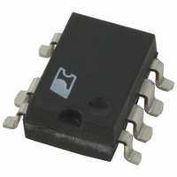
8-SMD Gull Wing, 7 Leads
Output Voltage
5.8 V
Input / Supply Voltage (max)
265 VAC
Input / Supply Voltage (min)
85 VAC
Duty Cycle (max)
63 %
Switching Frequency
200 KHz
Supply Current
280 uA
Operating Temperature Range
- 40 C to + 150 C
Mounting Style
SMD/SMT
Lead Free Status / RoHS Status
Lead free / RoHS Compliant
Available stocks
Company
Part Number
Manufacturer
Quantity
Price
Company:

Part Number:
LNK354GN
Manufacturer:
POWER
Quantity:
15 000


Figure 2. Functional Block Diagram.
Pin Functional Description
DRAIN (D) Pin:
Power MOSFET drain connection. Provides internal operating
current for both start-up and steady-state operation.
BYPASS (BP) Pin:
Connection point for a 0.1 µF external bypass capacitor for the
internally generated 5.8 V supply.
FEEDBACK (FB) Pin:
During normal operation, switching of the power MOSFET is
controlled by this pin. MOSFET switching is terminated when
a current greater than 49 µA is delivered into this pin.
SOURCE (S) Pin:
This pin is the power MOSFET source connection. It is also the
ground reference for the BYPASS and FEEDBACK pins.
2
FEEDBACK
LNK353/354
BYPASS
(FB)
(BP)
F
2/05
1.65 V -V
T
6.3 V
OSCILLATOR
JITTER
COUNTER
RESTART
CLOCK
AUTO-
DC
CLOCK
RESET
MAX
PRESENT
FAULT
4.85 V
5.8 V
Figure 3. Pin Configuration.
SHUTDOWN
THERMAL
+
-
S
R
BYPASS PIN
UNDER-VOLTAGE
Q
Q
BP
FB
G Package (SMD-8B)
P Package (DIP-8B)
S
S
REGULATOR
1
2
3
4
5.8 V
CURRENT LIMIT
COMPARATOR
BLANKING
LEADING
EDGE
8
7
5
+
-
S
D
S
V I
LIMIT
PI-2367-021105
PI-3491-111903
SOURCE
DRAIN
(D)
(S)
Related parts for LNK354GN
Image
Part Number
Description
Manufacturer
Datasheet
Request
R

Part Number:
Description:
Enhanced, Energy Ef?cient, Low Power Off-line Switcher Ic
Manufacturer:
Power Integrations, Inc.
Datasheet:

Part Number:
Description:
SOP-16
Manufacturer:
Power Integrations
Datasheet:
Part Number:
Description:
DIP8
Manufacturer:
Power Integrations
Datasheet:
Part Number:
Description:
TO-263
Manufacturer:
Power Integrations
Datasheet:
Part Number:
Description:
TO-263
Manufacturer:
Power Integrations
Datasheet: