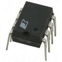
TOP209P Power Integrations, TOP209P Datasheet

TOP209P
Specifications of TOP209P
Available stocks
Related parts for TOP209P
TOP209P Summary of contents
Page 1
... Wide-Range DC Input Figure 1. Typical Application. ORDER PART NUMBER TOP209P TOP209G TOP210PFI TOP210G protection circuitry. Compared to discrete MOSFET and controller or self oscillating (RCC) switching converter solutions, a TOPSwitch integrated circuit can reduce total cost, component count, size, weight and at the same time increase efficiency and system reliability ...
Page 2
TOP209/210 V C CONTROL Z C SHUNT REGULATOR/ ERROR AMPLIFIER - + I FB OSCILLATOR D MAX CLOCK SAW R E Figure 2. Functional Block Diagram. Pin Functional Description 2 DRAIN Pin: Output MOSFET drain connection. Provides internal bias current ...
Page 3
TOPSwitch Family Functional Description TOPSwitch is a self biased and protected linear control current-to-duty cycle converter with an open drain output. High efficiency is achieved through the use of CMOS and integration of the maximum number of functions possible. CMOS ...
Page 4
TOP209/210 TOPSwitch Family Functional Description (cont.) The first time V reaches the upper threshold, the high-voltage C current source is turned off and the PWM modulator and output transistor are activated, as shown in Figure 5(a). During normal operation (when ...
Page 5
DRAIN 0 V OUT 0 I OUT Figure 6. Typical Waveforms for (1) Normal Operation, (2) Auto-restart. Shutdown/Auto-restart To minimize TOPSwitch power dissipation, the shutdown/ auto-restart circuit turns the ...
Page 6
TOP209/210 General Circuit Description Figure 7 shows a low-cost, DC input, flyback switching power supply using the TOP210 integrated circuit. This power supply operates from a DC voltage derived from rectified and filtered AC mains voltage ...
Page 7
BR1 + DFO6M RA 470 k - JP1* JUMPER 470 k 200 min. 0.2A C6 47nF 250VAC Figure 8. Schematic Diagram ...
Page 8
TOP209/210 Key Application Considerations Use a Kelvin connection to the SOURCE pin for the CONTROL pin bypass capacitor as shown in Figure 9. Minimize peak voltage and ringing on the DRAIN voltage at turn-off. Use a Zener or TVS Zener ...
Page 9
DRAIN Voltage ........................................... - 0.3 to 700 V CONTROL Voltage ..................................... - 0 CONTROL Current ............................................... 100 mA 1. Unless noted, all voltages referenced to SOURCE Parameter Symbol CONTROL FUNCTIONS Output ...
Page 10
TOP209/210 Parameter Symbol SHUTDOWN/AUTO-RESTART (cont.) UV Lockout Threshold Voltage Auto-restart Hysteresis Voltage Auto-restart Duty Cycle Auto-restart Frequency CIRCUIT PROTECTION Self-protection Current Limit Leading Edge Blanking Time Current Limit Delay Thermal Shutdown Temperature Thermal Shutdown 2 Hysteresis Power-up Reset V Threshold ...
Page 11
Parameter Symbol OUTPUT ON-State R Resistance DS(ON) OFF-State I Current DSS Breakdown BV Voltage DSS Rise t Time R Fall t Time F DRAIN Supply Voltage SUPPLY Shunt Regulator V Voltage C(SHUNT) Shunt Regulator Temperature Drift I CD1 CONTROL Supply/ ...
Page 12
TOP209/210 NOTES: (continued) i. The 470 5 W load resistor at the DRAIN pin should be shorted. S1 & S2 should stay closed. ii. The 40 V output supply should be replaced with a curve tracer capable of forcing 700 ...
Page 13
BENCH TEST PRECAUTIONS FOR EVALUATION OF ELECTRICAL CHARACTERISTICS The following precautions should be followed when testing TOPSwitch by itself outside a power supply. The schematic shown in Figure 12 is suggested for laboratory testing of TOPSwitch. When the DRAIN supply ...
Page 14
TOP209/210 Typical Performance Characteristics (cont.) OUTPUT CHARACTERISTIC 300 TCASE=25 C 250 TCASE=100 C 200 150 100 DRAIN Voltage ( 8/ DRAIN CAPACITANCE POWER ...
Page 15
DIM inches mm A 0.370-0.385 9.40-9.78 B 0.245-0.255 6.22-6.48 C 0.125-0.135 3.18-3.43 G 0.015-0.040 0.38-1.02 H 0.120-0.135 3.05-3.43 J1 0.060 (NOM) 1.52 (NOM) J2 0.014-0.022 0.36-0.56 K 0.010-0.012 0.25-0.30 L 0.090-0.110 2.29-2.79 M 0.030 (MIN) 0.76 (MIN) N 0.300-0.320 7.62-8.13 ...
Page 16
... Power Integrations reserves the right to make changes to its products at any time to improve reliability or manufacturability. Power Integrations does not assume any liability arising from the use of any device or circuit described herein, nor does it convey any license under its patent rights or the rights of others. ...


