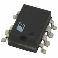
LNK500G Power Integrations, LNK500G Datasheet - Page 10

LNK500G
Manufacturer Part Number
LNK500G
Description
IC SWIT OCP CV/CC HV 8SMD
Manufacturer
Power Integrations
Series
LinkSwitch®r
Datasheet
1.LNK500PN.pdf
(20 pages)
Specifications of LNK500G
Output Isolation
Isolated
Frequency Range
24 ~ 49.5kHz
Voltage - Output
700V
Power (watts)
5.5W
Operating Temperature
-40°C ~ 150°C
Package / Case
8-SMD Gull Wing, 7 Leads
Lead Free Status / RoHS Status
Contains lead / RoHS non-compliant
Available stocks
Company
Part Number
Manufacturer
Quantity
Price
Company:
Part Number:
LNK500GN
Manufacturer:
Power Integrations
Quantity:
135
Company:
Part Number:
LNK500GN
Manufacturer:
POWER
Quantity:
15 000
Part Number:
LNK500GN
Manufacturer:
POWER
Quantity:
20 000
Part Number:
LNK500GN-TL
Manufacturer:
POWER
Quantity:
20 000
Quick Design Checklist
As with any power supply design, all LinkSwitch designs
should be verified on the bench to make sure that component
specifications are not exceeded under worst case conditions.
Note: In a LinkSwitch circuit, the SOURCE is a switching
node. This should be taken into consideration during testing.
Oscilloscope measurements should be made with probe grounded
to DC voltages such as primary return or DC rail but not to
SOURCE. Power supply input voltage should always be supplied
using an isolation transformer. The following minimum set of
tests is strongly recommended:
1. Maximum drain voltage – Verify that V
2. Maximum drain current – At maximum ambient temperature,
Figure 11. Recommended Circuit Board Layout for LinkSwitch using P Package.
10
675 V at highest input voltage and peak output power.
maximum input voltage and peak output power, verify drain
current waveforms at start-up for any signs of transformer
saturation and excessive leading edge current spikes.
LinkSwitch has a minimum leading edge blanking time of
200 ns to prevent premature termination of the on-cycle.
Verify that the leading edge current spike event is below
current limit at the end of the 200 ns blanking period.
LNK500
D
2/05
Capacitor
Output
Transformer
Capacitor
Y1-
DS
DC Out
does not exceed
-
+
C
S
LinkSwitch
S
S
3. Thermal check – At peak output power, minimum input
4. Centered output characteristic – Using a transformer with
Design Tools
Up to date information on design tools can be found at the
Power Integrations website: www.powerint.com.
S
voltage and maximum ambient temperature, verify that the
temperature specifications are not exceeded for LinkSwitch,
transformer, output diode and output capacitors. Enough
thermal margin should be allowed for part-to-part variation of
the R
low line, peak power, a maximum LinkSwitch SOURCE pin
temperature of 100 °C is recommended to allow for these
variations.
nominal primary inductance and at an input voltage midway
between low and high line, verify that the peak power point
occurs at the desired nominal output current, with the correct
output voltage. If this does not occur then the design should
be refined to ensure the overall tolerance limits are met.
DS(ON)
D
S
of LinkSwitch as specified in the data sheet. Under
Input Filter
Capacitor
PI-2900-070202
HV DC
+
-
Input


