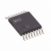
DS2762BE+025/T&R Maxim Integrated Products, DS2762BE+025/T&R Datasheet - Page 10

DS2762BE+025/T&R
Manufacturer Part Number
DS2762BE+025/T&R
Description
IC MON BATT LI-ION HP 16-TSSOP
Manufacturer
Maxim Integrated Products
Datasheet
1.DS2762BE025TR.pdf
(25 pages)
Specifications of DS2762BE+025/T&R
Function
Battery Monitor
Battery Type
Lithium-Ion (Li-Ion)
Voltage - Supply
2.5 V ~ 5.5 V
Operating Temperature
-40°C ~ 85°C
Mounting Type
Surface Mount
Package / Case
16-TSSOP
Lead Free Status / RoHS Status
Lead free / RoHS Compliant
Other names
DS2762BE+025/T&R
DS2762BE+025/TR
DS2762BE+025/TR
register, and enters sleep mode. The DS2762 provides a current-limited (I
V
reaches 3V (typ), the DS2762 returns to normal operation, awaiting connection of a charger to turn on the charge
FET and pull out of sleep mode.
Overcurrent, Charge Direction. The voltage difference between the IS1 pin and the IS2 pin (V
filtered voltage drop across the current-sense resistor. If V
than overcurrent delay t
register. The charge current path is not re-established until the voltage on the PLS pin drops below V
DS2762 provides a test current of value I
offending charge current source.
Overcurrent, Discharge Direction. If V
external discharge FET and sets the DOC flag in the protection register. The discharge current path is not re-
established until the voltage on PLS rises above V
V
Short Circuit. If the voltage on the SNS pin with respect to V
longer than short-circuit delay t
protection register. The discharge current path is not re-established until the voltage on PLS rises above V
The DS2762 provides a test current of value I
circuit.
Figure 3. Li+ Protection Circuitry Example Waveforms
Summary. All of the protection conditions described above are ORed together to affect the CC and DC outputs.
DD
DD
DISCHARGE
to PLS to pull PLS up to detect the removal of the offending low-impedance load.
to gently charge severely depleted cells. The recovery path is enabled when 0 £ V
SLEEP
CHARGE
DC = (Undervoltage) or (Overcurrent, Either Direction) or (Short Circuit) or (Protection Register Bit DE = 0)
CC = (Overvoltage) or (Undervoltage) or (Overcurrent, Charge Direction) or (Protection Register bit CE = 0)
MODE
NOTE 1: TO ALLOW THE DEVICE TO REACT QUICKLY TO SHORT CIRCUITS, DETECTION OCCURS ON THE SNS PIN RATHER THAN ON THE
FILTERED IS1 AND IS2 PINS. THE ACTUAL SHORT-CIRCUIT DETECT CONDITION IS V
V
CELL
or (Sleep Mode)
or (Sleep Mode)
CC
DC
V
IS
t
OVD
OCD
, the DS2762 shuts off both external FETs and sets the COC flag in the protection
t
SCD
SCD
, the DS2762 shuts off the external discharge FET and sets the DOC flag in the
(NOTE 1)
IS
is less than -V
t
TST
OVD
TST
from PLS to V
from V
DD
t
10 of 25
OCD
- V
DD
OC
TP
IS
. The DS2762 provides a test current of value I
to PLS to pull PLS up to detect the removal of the short
for a period longer than t
exceeds overcurrent threshold V
SS
SS
t
OCD
to pull PLS down to detect the removal of the
exceeds short-circuit threshold V
SNS
> V
RC
SC
) recovery charge path from PLS to
.
OCD
t
UVD
, the DS2762 shuts off the
DD
< 3V (typ). Once V
OC
IS
for a period longer
= V
SC
IS1
DD
-V
V
V
V
V
V
-V
V
V
V
ACTIVE
INACTIVE
for a period
0
- V
SS
OV
CE
UV
OC
PLS
SS
DD
OC
SC
- V
IS2
DD
TST
TP
) is the
- V
. The
from
TP
DD
.


