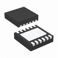
LT3650EDD-4.2#TRPBF Linear Technology, LT3650EDD-4.2#TRPBF Datasheet - Page 17

LT3650EDD-4.2#TRPBF
Manufacturer Part Number
LT3650EDD-4.2#TRPBF
Description
IC CHARGER LI-ION 4.1V 2A 12-DFN
Manufacturer
Linear Technology
Type
Battery Chargerr
Datasheet
1.LT3650EDD-4.2PBF.pdf
(20 pages)
Specifications of LT3650EDD-4.2#TRPBF
Function
Charge Management
Battery Type
Lithium-Ion (Li-Ion), Lithium-Polymer (Li-Pol)
Voltage - Supply
4.75 V ~ 32 V
Operating Temperature
-40°C ~ 85°C
Mounting Type
Surface Mount
Package / Case
12-WFDFN Exposed Pad
Output Voltage
4.2V
Operating Supply Voltage (min)
4.75V
Operating Temp Range
-40C to 85C
Mounting
Surface Mount
Pin Count
12
Operating Temperature Classification
Industrial
Lead Free Status / RoHS Status
Lead free / RoHS Compliant
Available stocks
Company
Part Number
Manufacturer
Quantity
Price
Layout Considerations
The LT3650 switch node has rise and fall times that are
typically less than 10ns to maximize conversion effi ciency.
The switched node (Pin SW) trace should be kept as short
as possible to minimize high frequency noise. The input
capacitor (C
this switching noise. Short, wide traces on these nodes
also help to avoid voltage stress from inductive ringing.
The BOOST decoupling capacitor should also be in close
proximity to the IC to minimize inductive ringing. The
SENSE and BAT traces should be routed together and
kept as short as possible. Shielding these signals from
switching noise with ground is recommended.
High current paths and transients should be kept iso-
lated from battery ground, to assure an accurate output
voltage reference. Effective grounding can be achieved
by considering switched current in the ground plane,
and careful component placement and orientation can
APPLICATIONS INFORMATION
IN
) should be placed close to the IC to minimize
Figure 9. Component Orientation Isolates High Current Paths From Sensitive Nodes
1
C
IN
V
IN
LT3650
SENSE
BAT
SW
2
D
F
C
BAT
effectively steer these high currents such that the battery
reference does not get corrupted. Figure 9 illustrates an
effective grounding scheme using component placement
to control ground currents. When the switch is enabled
(loop #1), current fl ows from the input bypass capacitor
(C
tive terminal. When the switch is disabled (loop #2), the
current to the battery positive terminal is provided from
ground through the freewheeling Schottky diode (D
both cases, these switched currents return to ground via
the output bypass capacitor (C
The LT3650 packaging has been designed to effi ciently
remove heat from the IC via the Exposed Pad on the
backside of the package, which is soldered to a copper
footprint on the PCB. This footprint should be made as
large as possible to reduce the thermal resistance of the
IC case to ambient air.
IN
) through the switch and inductor to the battery posi-
R
SENSE
LT3650-4.1/LT3650-4.2
365042 F09
V
+
BAT
BAT
).
17
36504142fb
F
). In


