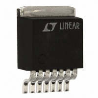
LT1513CR Linear Technology, LT1513CR Datasheet - Page 10

LT1513CR
Manufacturer Part Number
LT1513CR
Description
IC BATT CHRGR CONST/PROG I/V 7DD
Manufacturer
Linear Technology
Datasheet
1.LT1513-2CR.pdf
(16 pages)
Specifications of LT1513CR
Function
Charge Management
Battery Type
All Battery Types
Voltage - Supply
2.7 V ~ 25 V
Operating Temperature
0°C ~ 125°C
Mounting Type
Surface Mount
Package / Case
TO-263-8, D²Pak (7 leads + Tab), TO-263CA
Lead Free Status / RoHS Status
Contains lead / RoHS non-compliant
Available stocks
Company
Part Number
Manufacturer
Quantity
Price
Company:
Part Number:
LT1513CR
Manufacturer:
LT
Quantity:
5 510
Part Number:
LT1513CR
Manufacturer:
LT/凌特
Quantity:
20 000
Company:
Part Number:
LT1513CR#PBF
Manufacturer:
MCSM
Quantity:
7 031
Part Number:
LT1513CR#PBF
Manufacturer:
LINEAR/凌特
Quantity:
20 000
Part Number:
LT1513CR#TRPBF
Manufacturer:
LINEAR/凌特
Quantity:
20 000
APPLICATIONS
LT1513/LT1513-2
Programmed Charging Current
LT1513-2 charging current can be programmed with a DC
voltage source or equivalent PWM signal, as shown in
Figure 5. In constant-current mode, I
ground. The I
voltage across R4 in the ratio R4/R5.
Charging current is given by:
I
I
wide range of program currents. The voltage across R3 at
maximum charge current can be increased to reduce
offset errors at lower charge currents. In Figure 5, I
from 0V to 5V corresponds to an I
+37/– 62mA. C4 and R4 smooth the switch current wave-
form. During constant-current operation, the voltage feed-
back network loads the FB pin, which is held at V
I
10
FB
FB
FB
I
input current is small and can normally be ignored, but
CHARGE
offset voltage must be considered if operating over a
amplifier. It is recommended that this load does not
V
SET
(
C
V
R5
330
ISET
C5
0.1 F
voltage across R5 is balanced by the
THIS IS A SIMPLIFIED AC MODEL FOR THE LT1513 IN CONSTANT-
VOLTAGE MODE. RESISTOR AND CAPACITOR NUMBERS
CORRESPOND TO THOSE USED IN FIGURE 1. R
THE PHASE DELAY IN THE MODULATOR. C3 IS 3pF FOR A 10 H
INDUCTOR. IT SHOULD BE SCALED PROPORTIONALLY FOR OTHER
INDUCTOR VALUES (6pF FOR 20 H). THE MODULATOR IS A
TRANSCONDUCTANCE WHOSE GAIN IS A FUNCTION OF INPUT AND
BATTERY VOLTAGE AS SHOWN.
U
** R
)(
* FOR 8.4V BATTERY. ADJUST VALUE OF R1 FOR ACTUAL BATTERY VOLTAGE
R R
P
4
INFORMATION
AND C
R
U
/
C
3pF
P
3
**
5
P
)–
MODEL PHASE DELAY IN THE MODULATOR
R
1M
R
330k
P
V1
G
**
I
FBVOS
W
g
V
V
m
CHARGE
IN
BAT
1500 mho
FB
=
MODULATOR SECTION
= DC INPUT VOLTAGE
Figure 6. Constant-Voltage Small-Signal Model
g
= DC BATTERY VOLTAGE
V1
I
m
P
acts as a virtual
EA
=
V
IN
–
+
4(V
of 0A to 1A
+ V
IN
U
REF
BAT
)
P
AND C
1.245V
by the
SET
P
MODEL
I
P
FB
exceed 60 A to maintain a sharp constant voltage to
constant current crossover characteristic. I
also be controlled by a PWM input. Assuming the signal is
a CMOS rail-to-rail output with a source impedance of less
than a few hundred ohms, effective I
by the PWM ratio. I
entire 0% to 100% range.
Voltage Mode Loop Stability
The LT1513 operates in constant-voltage mode during the
final phase of charging lithium-ion and lead-acid batteries.
This feedback loop is stabilized with a series resistor and
capacitor on the V
simplified model for the voltage loop. The error amplifier is
modeled as a transconductance stage with g
AS SHOWN, THIS LOOP HAS A UNITY-GAIN FREQUENCY OF
ABOUT 250Hz. UNITY-GAIN WILL MOVE OUT TO SEVERAL
KILOHERTZ IF BATTERY RESISTANCE INCREASES TO SEVERAL
OHMS. R5 IS NOT USED IN ALL APPLICATIONS, BUT IT GIVES
BETTER PHASE MARGIN IN CONSTANT-VOLTAGE MODE WITH
HIGH BATTERY RESISTANCE.
R1*
71.5k
R2
12.5k
C1
+
I
SET
C
+
CHARGE
pin of the chip. Figure 6 shows the
249k
R5
C1
LT1513-2
Figure 5
R
EACH
C1
22 F
EACH
CAP
0.15
I
FB
has good linearity over the
C4
0.1 F
10k
R4
1513 F05
SET
R3
0.2
L1B
BATTERY
R
0.1
BAT
is V
1513 F06
m
CC
= 1500 mho
CHARGE
multiplied
sn1513 1513fas
can


