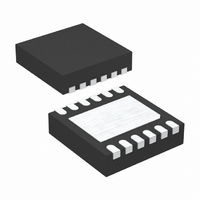
LT3650EDD-8.2#PBF Linear Technology, LT3650EDD-8.2#PBF Datasheet - Page 7

LT3650EDD-8.2#PBF
Manufacturer Part Number
LT3650EDD-8.2#PBF
Description
IC PWR MANAGER/CHRGR 12-DFN
Manufacturer
Linear Technology
Datasheet
1.LT3650EDD-8.4PBF.pdf
(20 pages)
Specifications of LT3650EDD-8.2#PBF
Function
Charge Management
Battery Type
Lithium-Ion (Li-Ion), Lithium-Polymer (Li-Pol)
Voltage - Supply
9 V ~ 32 V
Operating Temperature
-40°C ~ 85°C
Mounting Type
Surface Mount
Package / Case
12-WFDFN Exposed Pad
Input Voltage
32V
No. Of Outputs
1
Supply Voltage Range
9V To 32V
No. Of Pins
12
Operating Temperature Range
-40°C To +85°C
Msl
MSL 1 - Unlimited
Termination Type
SMD
Supply Voltage Min
9V
Rohs Compliant
Yes
Filter Terminals
SMD
Frequency
1MHz
Lead Free Status / RoHS Status
Lead free / RoHS Compliant
Available stocks
Company
Part Number
Manufacturer
Quantity
Price
charge current) is the desired soft-start interval (t
no R
The RNG/SS pin is pulled low during fault conditions,
allowing graceful recovery from faults should soft-start
functionality be implemented. Both the soft-start capaci-
tor and the programming resistor can be implemented in
parallel. All C/10 monitoring functions are disabled while
V
intervals.
RNG/SS voltage can also be manipulated using an active
device, employing a pulldown transistor to disable charge
current or to dynamically servo maximum charge current.
Manipulation of the RNG/SS pin with active devices that
have low impedance pull-up capability is not allowed (see
the Applications Information section).
NTC (Pin 8): Battery Temperature Monitor Pin. This pin is
the input to the NTC (Negative Temperature Coeffi cient)
thermistor temperature monitoring circuit. This function is
enabled by connecting a 10kΩ, B = 3380 NTC thermistor
from the NTC pin to ground. The pin sources 50μA, and
monitors the voltage across the 10kΩ thermistor. When the
voltage on this pin is above 1.36V (T < 0°C) or below 0.29V
(T > 40°C), charging is disabled and the CHRG andFAULT
pins are both pulled low. If internal timer termination is
being used, the timer is paused, suspending the charg-
ing cycle. Charging resumes when the voltage on NTC
returns to within the 0.29V to 1.36V active region. There
is approximately 5°C of temperature hysteresis associated
with each of the temperature thresholds. The temperature
monitoring function remains enabled while thermistor
resistance to ground is less than 250kΩ, so if this function
is not desired, leave the NTC pin unconnected.
BAT (Pin 9): Battery Voltage Monitor Pin. Connect 10μF
decoupling capacitance (C
Depending on application requirements, larger value
decoupling capacitors may be required (see the Applica-
tion Information section). The charge function operates to
achieve the fi nal fl oat voltage at this pin. The auto-restart
feature initiates a new charging cycle when the voltage at
PIN FUNCTIONS
RNG/SS
C
RNG SS
RNG/SS
/
is below 0.1V to accommodate long soft-start
, this capacitor value follows the relation:
= 50μ
A t
•
SS
BAT
) from this pin to ground.
SS
). For
the BAT pin falls 2.5% below this fl oat voltage. Once the
charge cycle is terminated, the input bias current of the
BAT pin is reduced to <0.1μA, to minimize battery discharge
while the charger remains connected.
SENSE (Pin 10): Charge Current Sense Pin. Connect the
more positive voltage end of the inductor sense resistor
(R
pin. The voltage across this resistor sets the average
charge current. The maximum average charge current
(I
This resistor can be set to program maximum charge
currents as high as 2A. The sense resistor value follows
the relation:
Once the charge cycle is terminated, the input bias current
of the SENSE pin is reduced to <0.1μA, to minimize battery
discharge while the charger remains connected.
BOOST (Pin 11): Bootstrapped Supply Rail for Switch
Drive. This pin facilitates saturation of the switch transistor.
Connect a 1μF or greater capacitor from the BOOST pin
to the SW pin. Operating range of this pin is 0V to 8.5V,
referenced to the SW pin. The voltage on the decoupling
capacitor is refreshed through a rectifying diode, with
the anode connected to either the battery output voltage
or an external source, and the cathode connected to the
BOOST pin.
SW (Pin 12): Switch Output Pin. This pin is the output
of the charger switch, and corresponds to the emitter of
the switch transistor. When enabled, the switch shorts
the SW pin to the V
switch is bootstrapped above the V
BOOST supply pin, allowing saturation of the switch for
maximum effi ciency. The effective on-resistance of the
boosted switch is 0.175Ω.
SGND (Pin 13): Ground Reference and Backside Exposed
Lead Frame Thermal Connection. Solder the exposed lead
frame to the PCB ground plane.
MAX
SENSE
R
SENSE
) corresponds to 100mV across the sense resistor.
) to the SENSE pin and the other end to the BAT
=
LT3650-8.2/LT3650-8.4
I
0 1 .
MAX
V
IN
supply. The drive circuitry for this
IN
supply using the
36508284fc
7


