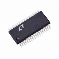
LTC1960CG#TR Linear Technology, LTC1960CG#TR Datasheet - Page 15

LTC1960CG#TR
Manufacturer Part Number
LTC1960CG#TR
Description
IC BATT CHRGR/SELECTR DUAL36SSOP
Manufacturer
Linear Technology
Type
Battery Chargerr
Specifications of LTC1960CG#TR
Function
Charge Management
Voltage - Supply
6 V ~ 28 V
Operating Temperature
0°C ~ 70°C
Mounting Type
Surface Mount
Package / Case
36-SSOP (0.200", 5.30mm Width)
Operating Supply Voltage (min)
6V
Operating Supply Voltage (max)
28V
Operating Temp Range
0C to 70C
Package Type
SSOP
Mounting
Surface Mount
Pin Count
36
Operating Temperature Classification
Commercial
Lead Free Status / RoHS Status
Contains lead / RoHS non-compliant
Lead Free Status / RoHS Status
Contains lead / RoHS non-compliant
Other names
LTC1960CGTR
Available stocks
Company
Part Number
Manufacturer
Quantity
Price
OPERATION
Battery Charger Controller
The LTC1960 charger controller uses a constant off-time,
current mode step-down architecture. During normal
operation, the top MOSFET is turned on each cycle when
the oscillator sets the SR latch and turned off when the
main current comparator ICMP resets the SR latch. While
the top MOSFET is off, the bottom MOSFET is turned on
until either the inductor current reverses, as indicated by
current comparator IREV, or the beginning of the next
cycle. The oscillator uses the equation:
to set the bottom MOSFET on time. The peak inductor
current at which ICMP resets the SR latch is controlled
by the voltage on I
loops, depending upon the situation at hand. The average
current control loop converts the voltage between CSP and
CSN to a representative current. Error amp CA2 compares
this current against the desired current requested by the
IDAC at the I
is satisfied. The BAT1/BAT2 MUX provides the selected
battery voltage at CHGMON, which is divided down to the
V
amp EA to decrease I
reference. The amplifier CL1 monitors and limits the input
current, normally from the AC adapter, to a preset level
(100mV/R
I
An overvoltage comparator, 0V, guards against transient
overshoots (>7%). In this case, the top MOSFET is turned
off until the overvoltage condition is cleared. This feature
is useful for batteries which “load dump” themselves by
opening their protection switch to perform functions such
as calibration or pulse mode charging.
Charging is inhibited for battery voltages below the mini-
mum charging threshold, V
when the low current mode of the IDAC is selected.
The top MOSFET driver is powered from a floating boot-
strap capacitor C
from V
is turned off. A 2µF to 4.7µF capacitor across V
is required to provide a low dynamic impedance to charge
TH
SET
t
voltage and thus reduce battery charging current.
OFF
pin by the VDAC resistor divider and is used by error
CC
=
through an external diode when the top MOSFET
CL
f
OSC
1
). At input current limit, CL1 will decrease the
SET
•
pin and adjusts I
B
(V
. This capacitor is normally recharged
TH
DCIN
TH
. I
V
if the V
TH
DCIN
− V
is in turn controlled by several
CHMIN
CSN
SET
. Charging is not inhibited
)
voltage is above the 0.8V
TH
until the IDAC value
CC
to GND
the boost capacitor. It is also required for stability and
power-on reset purposes.
As V
the converter will attempt to turn on the top MOSFET
continuously (“dropout’’). A dropout timer detects this
condition and forces the top MOSFET to turn off, and the
bottom MOSFET on, for about 200ns at 40µs intervals to
recharge the bootstrap capacitor.
Charge MUX Switches
The equivalent circuit of a charge MUX switch driver is
shown in Figure 3. If the charger controller is not enabled,
the charge MUX drivers will drive the gate and source of
the series-connected MOSFETs to a low voltage and the
switch is off. When the charger controller is on, the charge
MUX driver will keep the MOSFETs off until the voltage at
CSN rises at least 35mV above the battery voltage. GCH1
is then driven with an error amplifier EAC until the volt-
age between BAT1 and CSN satisfies the error amplifier
or until GCH1 is clamped by the internal Zener diode.
The time required to close the switch could be quite long
(many ms) due to the small currents output by the error
amp and depending upon the size of the MOSFET switch.
If the voltage at CSN decreases below V
comparator CC quickly turns off the MOSFETs to prevent
reverse current from flowing in the switches. In essence,
this system performs as a low forward voltage diode.
Operation is identical for BAT2.
CHARGER
BATTERY
FROM
TO
Figure 3. Charge MUX Switch Driver Equivalent Circuit
IN
1
decreases towards the selected battery voltage,
BAT1
CSN
35mV
20mV
(CHARGE PUMPED)
–
+
+
–
DCIN + 10V
CC
EAC
OFF
LTC1960
10k
BAT1
GCH1
SCH1
– 20mV, a
15
Q4
Q3
1960fb
1960 F03


