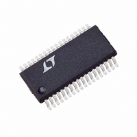
LTC1960CG#TR Linear Technology, LTC1960CG#TR Datasheet - Page 9

LTC1960CG#TR
Manufacturer Part Number
LTC1960CG#TR
Description
IC BATT CHRGR/SELECTR DUAL36SSOP
Manufacturer
Linear Technology
Type
Battery Chargerr
Specifications of LTC1960CG#TR
Function
Charge Management
Voltage - Supply
6 V ~ 28 V
Operating Temperature
0°C ~ 70°C
Mounting Type
Surface Mount
Package / Case
36-SSOP (0.200", 5.30mm Width)
Operating Supply Voltage (min)
6V
Operating Supply Voltage (max)
28V
Operating Temp Range
0C to 70C
Package Type
SSOP
Mounting
Surface Mount
Pin Count
36
Operating Temperature Classification
Commercial
Lead Free Status / RoHS Status
Contains lead / RoHS non-compliant
Lead Free Status / RoHS Status
Contains lead / RoHS non-compliant
Other names
LTC1960CGTR
Available stocks
Company
Part Number
Manufacturer
Quantity
Price
TGATE (Pin 32/Pin 21): Drives the top external MOSFET
of the battery charger buck converter.
SCH1 (Pin 33/Pin 22), SCH2 (Pin 36/Pin 25): Charger
MUX N-Channel Switch Source Returns. These two pins
are connected to the sources of the back-to-back switch
pairs, Q3/Q4 and Q9/Q10 (see Typical Application on back
page of data sheet), respectively. A small pull-down cur-
rent source returns these nodes to 0V when the switches
are turned off.
GCH1 (Pin 34/Pin 23), GCH2 (Pin 35/Pin 24): Charger
MUX N-Channel Switch Gate Drives. These two pins drive
the gates of the back-to-back switch pairs, Q3/Q4 and Q9/
Q10, between the charger output and the two batteries.
External Power Supply Pins
V
via four internal diodes to the DCIN, SCN, BAT1, and BAT2
pins. Bypass this pin with a 1µF to 2µF capacitor.
BAT1 (Pin 3/Pin 29), BAT2 (Pin 2/Pin 28): These two
pins are the inputs from the two batteries for power to
the LTC1960 and to provide voltage feedback to the bat-
tery charger.
LOPWR (Pin 12/Pin 38): LOPWR Comparator Input from
SCN External Resistor Divider to GND. If the voltage at
LOPWR is lower than the LOPWR comparator threshold,
then system power has failed and power is autonomously
switched to a higher voltage source, if available. See
PowerPath section of LTC1960 operation.
DCDIV (Pin 17/Pin 5): External DC Source Comparator
Input from DCIN External Resistor Divider to GND. If the
voltage at DCDIV is above the DCDIV comparator thresh-
old, then the DC bit is set and the wall adapter power is
considered to be adequate to charge the batteries. If DCDIV
rises more than 1.8V above V
switches are latched off until all power is removed.
A capacitor from DCDIV to GND is recommended to prevent
noise-induced false emergency turn-off conditions from
being detected. Refer to “Fast PowerPath Turn-Off” in the
Operation section and the Typical Application on the back
page of this data sheet.
PIN FUNCTIONS
PLUS
(Pin 1/Pin 27): Supply. The V
(G/UHF)
CC
, then all of the PowerPath
PLUS
pin is connected
DCIN (Pin 29/Pin 18): Supply. External DC power source.
A 1µF bypass capacitor should be connected to this pin as
close as possible. No series resistance is allowed, since
the adapter current limit comparator input is also this pin.
Internal Power Supply Pins
GND (Pin 16/Pin 4, Pin 10, Pin 26, Pin 39): Ground for
Low Power Circuitry.
PGND (Pin 26/Pin 15): High Current Ground Return for
BGATE Driver.
V
this output with at least a 2µF to 4.7µF capacitor. Do not
use this regulator output to supply more than 1mA to
external circuitry.
Digital Interface Pins
SSB (Pin 18/Pin 6): SPI Slave Select Input. Active low.
TTL levels. This signal is low when clocking data to/from
the LTC1960.
SCK (Pin 19/Pin 7): Serial SPI Clock. TTL levels.
MISO (Pin 20/Pin 8): SPI Master-In-Slave-Out Output,
Open Drain. Serial data is transmitted from the LTC1960,
when SSB is low, on the falling edge of SCK. TTL levels.
A 4.7k pull-up resistor is recommended.
MOSI (Pin 21/Pin 9): SPI Master-Out-Slave-In Input. Serial
data is transmitted to the LTC1960, when SSB is low, on
the rising edge of SCK. TTL levels.
GND (Exposed Pad Pin 39, UHF Package Only): Ground.
Must be soldered to the PCB ground for rated thermal
performance.
CC
(Pin 28/Pin 17): Internal Regulator Output. Bypass
LTC1960
1960fb
9


