ISL9209CIRZ Intersil, ISL9209CIRZ Datasheet
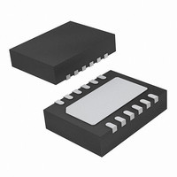
IC SAFETY SYSTEM CHARGER 12-TDFN

ISL9209CIRZ

Manufacturer Part Number
ISL9209CIRZ
Description
IC SAFETY SYSTEM CHARGER 12-TDFN
Manufacturer
Intersil
Datasheet

Specifications of ISL9209CIRZ

Function
Battery Monitor
Battery Type
Lithium-Ion (Li-Ion)
Voltage - Supply
4.3 V ~ 5.5 V
Operating Temperature
-40°C ~ 85°C
Mounting Type
Surface Mount
Package / Case
12-TDFN
Lead Free Status / RoHS Status
Lead free / RoHS Compliant
Charging System Safety Circuit
The ISL9209C is an integrated circuit (IC) optimized to
provide a redundant safety protection to a Li-ion battery from
failures of a charging system. The IC monitors the input
voltage, the battery voltage, and the charge current. When
any of the three parameters exceeds its limit, the IC turns off
an internal P-Channel MOSFET to remove the power from
the charging system. In addition to the above protected
parameters, the IC also monitors its own internal
temperature and turns off the P-Channel MOSFET when the
temperature exceeds +140°C. Together with the battery
charger IC and the protection module in a battery pack, the
charging system using the ISL9209C has triple-level
protection and is two-fault tolerant.
The IC is designed to turn on the internal PFET slowly to
avoid in-rush current at power-up but will turn off the PFET
quickly when the input is overvoltage in order to remove the
power before any damage occurs. The ISL9209C has a logic
warning output to indicate the fault and an enable input to
allow the system to remove the input power.
Ordering Information
*Add “-T” suffix for tape and reel. Please refer to TB347 for details on reel
specifications
NOTE: These Intersil Pb-free plastic packaged products employ special
Pb-free material sets, molding compounds/die attach materials, and
100% matte tin plate plus anneal (e3 termination finish, which is RoHS
compliant and compatible with both SnPb and Pb-free soldering
operations). Intersil Pb-free products are MSL classified at Pb-free peak
reflow temperatures that meet or exceed the Pb-free requirements of
IPC/JEDEC J STD-020.
Typical Application Circuit
PART NUMBER
ISL9209CIRZ*
(Note)
INPUT
R
C
ILIM
1
MARKING
09CZ
PART
VIN
ILIM
GND
ISL9209C
®
-40 to +85
RANGE
TEMP.
1
(°C)
WRN
OUT
VB
EN
Data Sheet
12 Ld 4x3 TDFN L12.4x3A
CHARGER
PACKAGE
BATTERY
ISL6292
(Pb-free)
R
VB
BATTERY
PACK
1-888-INTERSIL or 1-888-468-3774
DWG. #
PKG.
CAUTION: These devices are sensitive to electrostatic discharge; follow proper IC Handling Procedures.
Features
• Fully Integrated Protection Circuit for Three Protected
• High Accuracy Protection Thresholds
• User Programmable Overcurrent Protection Threshold
• Input Overvoltage Protection in Less Than 1µs
• High Immunity of False Triggering Under Transients
• Warning Output to Indicate the Occurrence of Faults
• Enable Input
• Easy to Use
• Thermal Enhanced TDFN Package
• Pb-Free (RoHS Compliant)
Applications
• Cell Phones
• Digital Still Cameras
• PDAs and Smart Phones
• Portable Instruments
• Desktop Chargers
Related Literature
• Technical Brief TB363 “Guidelines for Handling and
• Technical Brief TB379 “Thermal Characterization of
• Technical Brief TB389 “PCB Land Pattern Design and
Pinout
Variables
Processing Moisture Sensitive Surface Mount Devices
(SMDs)”
Packaged Semiconductor Devices”
Surface Mount Guidelines for QFN Packages”
January 16, 2009
All other trademarks mentioned are the property of their respective owners.
|
Intersil (and design) is a registered trademark of Intersil Americas Inc.
Copyright © Intersil Americas Inc. 2007, 2009. All Rights Reserved.
WRN
GND
VIN
VIN
NC
NC
1
2
3
4
6
5
(12 LD 4x3 TDFN)
TOP VIEW
ISL9209C
EPAD
12
10
11
9
8
7
ISL9209C
NC
OUT
OUT
ILIM
VB
EN
FN6489.1

Related parts for ISL9209CIRZ

ISL9209CIRZ Summary of contents

Page 1

... PART NUMBER PART RANGE (Note) MARKING (°C) ISL9209CIRZ* 09CZ -40 to +85 *Add “-T” suffix for tape and reel. Please refer to TB347 for details on reel specifications NOTE: These Intersil Pb-free plastic packaged products employ special Pb-free material sets, molding compounds/die attach materials, and ...

Page 2

... Thermal Resistance (Typical, Notes 2, 3) θ 4x3 TDFN Package . . . . . . . . . . . . . . . Maximum Junction Temperature (Plastic Package +150°C Maximum Storage Temperature Range . . . . . . . . . .-65°C to +150°C Pb-free Reflow Profile . . . . . . . . . . . . . . . . . . . . . . . . .see link below http://www.intersil.com/pbfree/Pb-FreeReflow.asp = 5.0V and T = +25°C, maximum and minimum values are guaranteed over IN A ...

Page 3

Pin Descriptions VIN (Pin 1, 2) The input power source. The VIN can withstand 30V input. GND (Pin 3) System ground reference. WRN (Pin 4) WRN is an open-drain logic output that turns LOW when any protection event occurs. NC ...

Page 4

Typical Operating Performance VIN (1V/DIV) VIN (1V/div) OUT (1V/div) OUT (1V/DIV) Load Current LOAD CURRENT (200mA/div) FIGURE 2. CAPTURED WAVEFORMS FOR POWER-UP. THE OUTPUT IS LOADED WITH A 10Ω RESISTOR Time: 500ms/div TIME: 500ms/DIV OUT (2V/div) OUT (2V/DIV) WRN (5V/DIV) ...

Page 5

Typical Operating Performance Time: 200ms/div TIME: 200ms/DIV FIGURE 8. POWER-UP WAVEFORMS WHEN OUTPUT IS SHORT-CIRCUITED 1000 900 800 700 600 500 400 300 200 100 INPUT VOLTAGE (V) FIGURE 10. INPUT BIAS CURRENT vs ...

Page 6

Typical Operating Performance 1040 CURRENT 1030 LIMIT = 1A 1020 4.3V 1010 1000 990 5.5V 980 970 -50 - TEMPERATURE (°C) FIGURE 14. OVERCURRENT PROTECTION THRESHOLDS vs TEMPERATURE AT VARIOUS INPUT VOLTAGES 520 CURRENT 515 4.3V LIMIT = ...

Page 7

Typical Operating Performance 2.0 1.8 1.6 1.4 1.2 1.0 0.8 0.6 0.4 0.2 0 -50 - TEMPERATURE (°C) FIGURE 20. EN INPUT THRESHOLD vs TEMPERATURE FIGURE 22. ON-RESISTANCE vs TEMPERATURE AT DIFFERENT INPUT VOLTAGES Theory of Operation The ...

Page 8

CP1 outputs a logic signal to turn off the power PFET within 1µs (see Figure 3) to prevent the high input voltage from damaging the electronics in the handheld system. The hysteresis for the input ...

Page 9

R Selection VB The R prevents a large current from the VB pin to the VB battery terminal, in case the ISL9209C fails. The recommended value should be between 200kΩ to 1MΩ. With 200kΩ resistance, the worst case current flowing ...

Page 10

... Intersil will have the FMEA document for the solution using the ISL9209C and the ISL6292C chip set but the layout FMEA should be added as part of the analysis ...

Page 11

... Accordingly, the reader is cautioned to verify that data sheets are current before placing orders. Information furnished by Intersil is believed to be accurate and reliable. However, no responsibility is assumed by Intersil or its subsidiaries for its use; nor for any infringements of patents or other rights of third parties which may result from its use ...

Related keywords