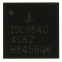
ISL6255AHRZ Intersil, ISL6255AHRZ Datasheet - Page 17

ISL6255AHRZ
Manufacturer Part Number
ISL6255AHRZ
Description
IC BATTERY CHRGR NOTEBOOK 28-QFN
Manufacturer
Intersil
Datasheet
1.ISL6255AHRZ.pdf
(22 pages)
Specifications of ISL6255AHRZ
Function
Charge Management
Battery Type
Lithium-Ion (Li-Ion), Lithium-Polymer (Li-Pol)
Voltage - Supply
7 V ~ 25 V
Operating Temperature
-10°C ~ 100°C
Mounting Type
Surface Mount
Package / Case
28-VFQFN Exposed Pad
Lead Free Status / RoHS Status
Lead free / RoHS Compliant
Available stocks
Company
Part Number
Manufacturer
Quantity
Price
Company:
Part Number:
ISL6255AHRZ
Manufacturer:
INTERSIL
Quantity:
400
gate current to prevent it from conduction, which is due to
the injected current into the drain-to-source parasitic
capacitor (Miller capacitor C
rising rate at phase node at the time instant of the high-side
MOSFET turning on; otherwise, cross-conduction problems
may occur. Reasonably slowing turn-on speed of the high-
side MOSFET by connecting a resistor between the BOOT
pin and gate drive supply source, and the high sink current
capability of the low-side MOSFET gate driver help reduce
the possibility of cross-conduction.
For the high-side MOSFET, the worst-case conduction
losses occur at the minimum input voltage:
The optimum efficiency occurs when the switching losses
equal the conduction losses. However, it is difficult to
calculate the switching losses in the high-side MOSFET
since it must allow for difficult-to-quantify factors that
influence the turn-on and turn-off times. These factors
include the MOSFET internal gate resistance, gate charge,
threshold voltage, stray inductance, pull-up and pull-down
resistance of the gate driver. The following switching loss
calculation provides a rough estimate.
Where Q
charge of the body-diode in low side MOSFET, I
valley current, I
are the peak gate-drive source/sink current of Q1, respectively.
To achieve low switching losses, it requires low drain-to-gate
charge Q
the higher the on-resistance. Therefore, there is a trade-off
between the on-resistance and drain-to-gate charge. Good
MOSFET selection is based on the Figure of Merit (FOM),
which is a product of the total gate charge and
on-resistance. Usually, the smaller the value of FOM, the
higher the efficiency for the same application.
For the low-side MOSFET, the worst-case power dissipation
occurs at minimum battery voltage and maximum input
voltage:
Choose a low-side MOSFET that has the lowest possible
on-resistance with a moderate-sized package like the SO-8
and is reasonably priced. The switching losses are not an
issue for the low side MOSFET because it operates at
zero-voltage-switching.
Choose a Schottky diode in parallel with low-side MOSFET
Q2 with a forward voltage drop low enough to prevent the
low-side MOSFET Q2 body-diode from turning on during the
P
P
P
Q
Q
Q
, 1
, 1
2
Switching
Conduction
=
⎛
⎜
⎜
⎝
1
gd
gd
−
: drain-to-gate charge, Q
V
. Generally, the lower the drain-to-gate charge,
V
=
OUT
IN
LP:
=
1
2
V
V
⎞
⎟
⎟
⎠
V
IN
Inductor peak current, I
OUT
I
IN
BAT
2
I
LV
I
R
f
s
BAT
2
DSON
I
, g
Q
gd
R
source
17
gd
), and caused by the voltage
DSON
rr
+
: total reverse recovery
1
2
V
IN
g,sink
I
LP
f
s
LV
and I
I
: inductor
, g
Q
sin
gd
g
ISL6255, ISL6255A
,
k
source
+
Q
rr
V
IN
f
s
dead time. This also reduces the power loss in the high-side
MOSFET associated with the reverse recovery of the
low-side MOSFET Q2 body diode.
As a general rule, select a diode with DC current rating equal
to one-third of the load current. One option is to choose a
combined MOSFET with the Schottky diode in a single
package. The integrated packages may work better in
practice because there is less stray inductance due to a
short connection. This Schottky diode is optional and may be
removed if efficiency loss can be tolerated. In addition,
ensure that the required total gate drive current for the
selected MOSFETs should be less than 24mA. So, the total
gate charge for the high-side and low-side MOSFETs is
limited by the following equation:
Where I
less than 24mA. Substituting I
into the previous equation yields that the total gate charge
should be less than 80nC. Therefore, the ISL6255,
ISL6255A easily drives the battery charge current up to 8A.
Input Capacitor Selection
The input capacitor absorbs the ripple current from the
synchronous buck converter, which is given by:
This RMS ripple current must be smaller than the rated RMS
current in the capacitor datasheet. Non-tantalum chemistries
(ceramic, aluminum, or OSCON) are preferred due to their
resistance to power-up surge currents when the AC adapter
is plugged into the battery charger. For Notebook battery
charger applications, it is recommend that ceramic
capacitors or polymer capacitors from Sanyo be used due to
their small size and reasonable cost.
Table 2 shows the component lists for the typical application
circuit in Figure 15.
Q
I
rms
C2, C4, C8 0.1 μ F/50V ceramic capacitor
C3, C7, C9 1 μ F/10V ceramic capacitor, Taiyo Yuden
GATE
C1, C10
PARTS
C11
C5
C6
D1
D2
=
I
GATE
BAT
≤
I
GATE
f
s
10 μ F/25V ceramic capacitor, Taiyo Yuden
TMK325 MJ106MY X5R (3.2x2.5x1.9mm)
LMK212BJ105MG
10nF ceramic capacitor
6.8nF ceramic capacitor
3300pF ceramic capacitor
30V/3A Schottky diode, EC31QS03L (optional)
100mA/30V Schottky Diode, Central Semiconductor
is the total gate drive current and should be
V
OUT
TABLE 2. COMPONENT LIST
PART NUMBERS AND MANUFACTURER
(
V
V
IN
IN
−
V
OUT
GATE
)
= 24mA and f
s
= 300kHz
May 23, 2006
FN9203.2


