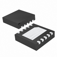
DS2746G+T&R Maxim Integrated Products, DS2746G+T&R Datasheet - Page 7

DS2746G+T&R
Manufacturer Part Number
DS2746G+T&R
Description
IC MON BATTERY 2-WIRE 10-TDFN
Manufacturer
Maxim Integrated Products
Datasheet
1.DS2746GTR.pdf
(17 pages)
Specifications of DS2746G+T&R
Function
Fuel, Gas Gauge/Monitor
Battery Type
Lithium-Ion (Li-Ion); Nickel-Metal Hydride (NiMH)
Voltage - Supply
2.5 V ~ 5.5 V
Operating Temperature
-40°C ~ 85°C
Mounting Type
Surface Mount
Package / Case
10-WFDFN Exposed Pad
Lead Free Status / RoHS Status
Lead free / RoHS Compliant
Figure 4. APPLICATION EXAMPLE
POWER MODES
The DS2746 operates in one of two power modes: active and sleep. While in active mode, the DS2746 operates as
a high-precision battery monitor with voltage, auxiliary inputs, current and accumulated current measurements
acquired continuously and the resulting values updated in the measurement registers. Read and write access is
allowed to all registers. In sleep mode, the DS2746 operates in a low-power mode with no measurement activity.
The DS2746 operating mode transitions from SLEEP to ACTIVE when:
The DS2746 operating mode transitions from ACTIVE to SLEEP when:
CAUTION: If SMOD = 1, a pull-up resistor is required on SCL and SDA in order to ensure that the DS2746
transitions from SLEEP to ACTIVE mode when the battery is charged. If the bus is not pulled up, the DS2746
remains in SLEEP and cannot accumulate the charge current.
MEASUREMENT SEQUENCE
The DS2746 uses seperate A/D converters to make voltage and current measurements. Each A/D converter
operates completely independent of the other, allowing measurements of voltage and current to be made in
parallel. Current Measurements are made at a resolution of 13 bits plus sign bit. The current register is updated
every 878ms with the average for that time period.
All Voltage Measurements are made at a resolution of 11 bits plus sign bit. The DS2746 continouly cycles through
measuring V
full sequence of voltage measurements requires 660ms to complete. V
before the AIN0 measurement time occurs. The V
sequence as long as the V
( SCL > V
SMOD = 1 AND [ ( SCL < V
(Li+/Polymer)
Protection IC
IN
1nF
, AIN0, and AIN1 in that order. Voltage measurement of each input requires 220ms to complete. A
IH
) OR ( SDA > V
1nF
ODIS
(V
OUT
IH
IL
Disable) bit is cleared. See Figure 5.
)
) AND ( SDA < V
PackID
Therm
Pack-
Pack+
(1) Optional for 8kV/15kV ESD
OUT
1K
1K
pin is enabled during the entire AIN0 and AIN1 measurement
7 of 17
IL
) ] for t
(1) 5.6V
SLEEP
10nF
150
VOUT
AIN0
AIN1
VSS
CTG
VDD
2.5V
DS2746
OUT
R
SNS
(1)
is active for a precharge time of t
SDA
SNS
SCL
VIN
1K
System
System
System
Serial
VDD
VSS
Bus
PRE


