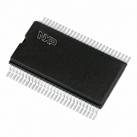
PCF8578T/1,112 NXP Semiconductors, PCF8578T/1,112 Datasheet - Page 15

PCF8578T/1,112
Manufacturer Part Number
PCF8578T/1,112
Description
IC LCD DRIVER DOT MATRIX 56-VSOP
Manufacturer
NXP Semiconductors
Specifications of PCF8578T/1,112
Package / Case
56-VSOP
Display Type
LCD
Configuration
Dot Matrix
Interface
I²C
Voltage - Supply
2.5 V ~ 6 V
Operating Temperature
-40°C ~ 85°C
Mounting Type
Surface Mount
Maximum Clock Frequency
3.3 KHz
Operating Supply Voltage
2.5 V to 6 V
Maximum Power Dissipation
400 mW
Maximum Operating Temperature
+ 150 C
Maximum Supply Current
50 mA
Minimum Operating Temperature
- 65 C
Lead Free Status / RoHS Status
Lead free / RoHS Compliant
Current - Supply
-
Digits Or Characters
-
Lead Free Status / Rohs Status
Details
Other names
568-3561-5
935278868112
PCF8578TD
935278868112
PCF8578TD
Philips Semiconductors
7.9
The configuration of the outputs (row or column) and the
selection of the appropriate driver waveforms are
controlled by the display mode controller.
7.10
The PCF8578 contains a 32
stores the display data. The RAM is divided into 4 banks
of 40 bytes (4
transferred to/from the RAM via the I
eight columns of data (0 to 7) cannot be displayed but
are available for general data storage and provide
compatibility with the PCF8579. There is a direct
correspondence between X-address and column output
number.
7.11
The addressing mechanism for the display RAM is
realized using the data pointer. This allows an individual
data byte or a series of data bytes to be written into, or read
from, the display RAM, controlled by commands sent on
the I
7.12
The storage and retrieval of display data is dependent on
the content of the subaddress counter. Storage takes
place only when the contents of the subaddress counter
agree with the hardware subaddress. The hardware
subaddress of the PCF8578, valid in mixed mode only, is
fixed at 0000.
7.13
The I
address, commands and display data bytes. It performs
the conversion of the data input (serial-to-parallel) and the
data output (parallel-to-serial). The PCF8578 acts as an
I
a slave receiver in row mode. A slave device cannot
control bus communication.
7.14
To enhance noise immunity in electrically adverse
environments, RC low-pass filters are provided on the
SDA and SCL lines.
2003 Apr 14
2
C-bus slave transmitter/receiver in mixed mode, and as
LCD row/column driver for
dot matrix graphic displays
2
2
C-bus.
C-bus controller detects the I
Display mode controller
Display RAM
Data pointer
Subaddress counter
I
Input filters
2
C-bus controller
8
40 bits). During RAM access, data is
40-bit static RAM which
2
C-bus protocol, slave
2
C-bus. The first
15
7.15
RAM operations are only possible when the PCF8578 is
in mixed mode.
In this event its hardware subaddress is internally fixed at
0000 and the hardware subaddresses of any PCF8579
used in conjunction with the PCF8578 must start at 0001.
There are three RAM ACCESS modes:
These modes are specified by bits G1 to G0 of the RAM
ACCESS command. The RAM ACCESS command
controls the order in which data is written to or read from
the RAM (see Fig.10).
To store RAM data, the user specifies the location into
which the first byte will be loaded (see Fig.11):
Subsequent data bytes will be written or read according to
the chosen RAM ACCESS mode. Device subaddresses
are automatically incremented between devices until the
last device is reached. If the last device has
subaddress 15, further display data transfers will lead to a
wrap-around of the subaddress to 0.
7.16
The display is generated by continuously shifting rows of
RAM data to the dot matrix LCD via the column outputs.
The number of rows scanned depends on the multiplex
rate set by bits M1 and M0 of the SET MODE command.
The display status (all dots on/off and normal/inverse
video) is set by bits E1 and E0 of the SET MODE
command. For bank switching, the RAM bank
corresponding to the top of the display is set by bits
B1 and B0 of the SET START BANK command. This is
shown in Fig.12. This feature is useful when scrolling in
alphanumeric applications.
7.17
The TEST pin must be connected to V
Character
Half-graphic
Full-graphic.
Device subaddress (specified by the DEVICE SELECT
command)
RAM X-address (specified by the LOAD X-ADDRESS
command)
RAM bank (specified by bits Y1 and Y0 of the RAM
ACCESS command).
RAM access
Display control
TEST pin
Product specification
SS
.
PCF8578


