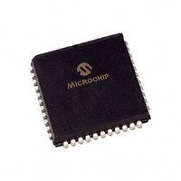
TC820CLW713 Microchip Technology, TC820CLW713 Datasheet - Page 13

TC820CLW713
Manufacturer Part Number
TC820CLW713
Description
IC ADC 3 3/4DGT LGC PROBE 44PLCC
Manufacturer
Microchip Technology
Datasheet
1.TC820CPL.pdf
(34 pages)
Specifications of TC820CLW713
Display Type
LCD
Configuration
7 Segment + 2 Annunciators
Digits Or Characters
A/D 3.75 Digits
Current - Supply
1mA
Voltage - Supply
9V
Operating Temperature
0°C ~ 70°C
Mounting Type
Surface Mount
Package / Case
44-PLCC
Lead Free Status / RoHS Status
Request inventory verification / Request inventory verification
Interface
-
Available stocks
Company
Part Number
Manufacturer
Quantity
Price
Company:
Part Number:
TC820CLW713
Manufacturer:
Microchip Technology
Quantity:
10 000
When the logic probe function is selected while FREQ/
VOLTS is low (A/D mode), the ADC will remain in the
Auto-Zero mode. The LCD will read "OL" and all
decimal points will be off
FIGURE 3-6:
If the logic probe is active while FREQ/VOLTS is high
(Counter mode), the frequency counter will continue to
operate. The display will read "OL" but the decimal
points will be visible. If the logic probe input is also
connected to the RANGE/FREQ input, bringing the
LOGIC input low will immediately display the frequency
at the logic probe input.
3.5
3.5.1
The TC820 is designed with true differential inputs, and
accepts input signals within the Input Stage Common
mode voltage (V
V
removed from the system when the TC820 operates
from a battery or floating power source (isolated from
measured system) and V
common (see
In systems where Common mode voltages exist, the
86 dB Common mode rejection ratio minimizes error.
Common mode voltages do, however, affect the
integrator output level. A worst case condition exists if
a large, positive V
scale, negative differential signal. The negative signal
drives the integrator output positive along with V
(Figure
output swing can be reduced below the recommended
2V full scale swing. The integrator output will swing
within 0.3V of V
error.
3.5.2
The TC820 reference, like the analog signal input, has
true differential inputs. In addition, the reference
voltage can be generated anywhere within the power
supply voltage of the converter. The differential
reference inputs permit ratiometric measurements and
simplify interfacing with sensors, such as load cells and
temperature sensors.
© 2007 Microchip Technology Inc.
** "Low" Annunciator and Buzzer will be on when DP0/LO = Logic High
DD
* "High" Annuciator will be on when DP1/HI = Logic High
– 1V to V
High
Low
3-6). For such applications, the integrator
Analog Pin Functional Description
DIFFERENTIAL SIGNAL INPUTS
(V
REFERENCE (V
*
**
IN
Figure
SS
+), (V
DD
+ 1.5V. Common mode voltages are
CM
CM
, or V
) range. The typical range is
3-5).
IN
LCD Reading.
exists in conjunction with a full
-)
DD
(Figure
SS
without increased linearity
is connected to analog
DD
).
, V
SS
)
CM
To prevent rollover type errors from being induced by
large Common mode voltages, C
compared to stray node capacitance. A 0.1 µF
capacitor is typical.
The TC820 offers a significantly improved analog
common temperature coefficient, providing a very
stable voltage suitable for use as a voltage reference.
The temperature coefficient of analog common is
typically 35 ppm/°C.
3.5.3
The analog common pin is set at a voltage potential
approximately 3.3V below V
between 3.15V and 3.45V below V
is tied internally to an N-channel FET capable of sink-
ing 3 mA. This FET will hold the common line at 3.3V
below V
common line toward V
current is limited to 12 µA, and is, therefore, easily
pulled to a more negative voltage (i.e., below V
3.3V).
The TC820 connects the internal V
to analog common during the auto-zero cycle. During
the reference integrate phase, V
analog common. If V
analog common, a Common mode voltage exists.
This is rejected by the converter's 86 dB Common
mode rejection ratio. In battery powered applications,
analog common and V
removing Common mode voltage concerns. In systems
where V
to a given voltage, analog common should be
connected to V
The analog common pin serves to set the analog
section reference or common point. The TC820 is
specifically designed to operate from a battery, or in
any “measurement" system where input signals are not
referenced (float), with respect to the TC820 power
source. The analog common potential of V
gives a 7V end of battery life voltage. The analog
common potential has a voltage coefficient of 0.001%.
With
(V
potential with excellent temperature stability (typically
35ppm/°C). This potential can be used to generate the
TC820
reference will be unnecessary in most cases, because
of the 35 ppm/°C temperature coefficient. See the
applications section for details.
DD
– V
a
DD
IN
SS
reference
- is connected to the power supply ground or
sufficiently
should an external load attempt to pull the
ANALOG COMMON
> 7V), analog common is a very stable
IN
-.
IN
voltage.
- is not externally connected to
high
DD
IN
. Analog common source
- are usually connected,
total
DD
An
REF
. This potential is
DD
IN
IN
- is connected to
DS21476C-page 13
external
. Analog common
+ and V
TC820
supply
should be large
DD
IN
- inputs
voltage
voltage
– 3.3V
DD
–


