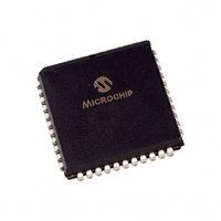
TC820CLW713 Microchip Technology, TC820CLW713 Datasheet - Page 19

TC820CLW713
Manufacturer Part Number
TC820CLW713
Description
IC ADC 3 3/4DGT LGC PROBE 44PLCC
Manufacturer
Microchip Technology
Datasheet
1.TC820CPL.pdf
(34 pages)
Specifications of TC820CLW713
Display Type
LCD
Configuration
7 Segment + 2 Annunciators
Digits Or Characters
A/D 3.75 Digits
Current - Supply
1mA
Voltage - Supply
9V
Operating Temperature
0°C ~ 70°C
Mounting Type
Surface Mount
Package / Case
44-PLCC
Lead Free Status / RoHS Status
Request inventory verification / Request inventory verification
Interface
-
Available stocks
Company
Part Number
Manufacturer
Quantity
Price
Company:
Part Number:
TC820CLW713
Manufacturer:
Microchip Technology
Quantity:
10 000
5.6.3
C
voltage swing without causing output saturation. Analog
common will normally supply the differential voltage
reference. For this case, a ±2V integrator output swing is
optimum when the analog input is near full scale. For 2.5
readings/second (F
0.22 µF value is suggested. If a different oscillator
frequency is used, C
proportion to maintain the nominal ±2V integrator
swing.
An exact expression for C
EQUATION 5-2:
C
rollover
recommended.
5.6.4
The input buffer amplifier and integrator are designed
with class A output stages. The integrator and buffer
can supply 40 µA drive currents with negligible linearity
errors. R
linear drive region, but not so large that printed circuit
board leakage currents induce errors. For a 400 mV
full-scale, R
5.7
A full-scale reading (4000 counts for TC820) requires
the input signal be twice the reference voltage. See
Reference Voltage Selection,
© 2007 Microchip Technology Inc.
Where:
INT
INT
F
R
V
should be selected to maximize integrator output
OSC
must have low dielectric absorption to minimize
V
INT
INT
FS
INT
Reference Voltage Selection
error.
INTEGRATING CAPACITOR - C
INTEGRATING RESISTOR - R
INT
is chosen to remain in the output stage
=
=
=
=
C
should be about 100 kΩ.
INT
A
OSC
=
Clock Frequency
Full-Scale Input Voltage
Integrating Resistor
Desired Full-Scale Integrator
Output Swing
INT
= 40 kHz) and V
polypropylene
V
INT
must be changed in inverse
INT
4000 V
R
is:
Table 5-1
INT
F
FS
OSC
FS
below.
capacitor
= 400 mV, a
INT
INT
is
TABLE 5-1:
In some applications, a scale factor other than unity
may exist between a transducer output voltage and the
required digital reading. Assume, for example, that a
pressure transducer output is 800 mV for 4000 lb/in
Rather than dividing the input voltage by two, the
reference voltage should be set to 400 mV. This per-
mits the transducer input to be used directly.
The internal voltage reference potential available at
analog common will normally be used to supply the
converter's reference voltage. This potential is stable
whenever the supply potential is greater than
approximately 7V. The low battery detection circuit and
analog common operate from the same internal
reference. This ensures that the low battery annunciator
will turn on at the time the internal reference begins to
lose regulation.
The TC820 can also operate with an external
reference.
erence applications.
FIGURE 5-7:
Connections.
Note 1:
Full Scale Input Voltage
(a) Internal Reference
SET V
V
TC820
SS
2V (Notes 3, 4)
Common
(V
REF
2:
3:
4:
Analog
9V
V
V
FS
REF
REF
200 mV
400 mV
V
= 1/2 V
+
) (Note 1)
DD
Figure 5-7
TC820 in A/D Converter mode, RANGE/
FREQ = logic low.
Not recommended.
V
mode range. See Section 3.2.7 “10:1
Range Change”.
Full-scale voltage values are not limited to
the values shown. For example, TC820
V
+
-
1V
FS
FS
V
2kΩ
22kΩ
REF
FULL SCALE
> 2V may exceed the Input Common
can be any value from 400 mV to 2V.
REFERENCE VOLTAGE
SELECTION
shows internal and external ref-
Reference Voltage
TC820
(Note 2)
Common
200 mV
500 mV
(b) External Reference
V
Analog
V
DD
V
V
1V
REF
REF
REF
+
-
DS21476C-page 19
TC820
MCP1525
Resolution
250 µV
500 µV
10 µV
—
1μF
V
OUT
V
V
V+
SS
IN
2
.


