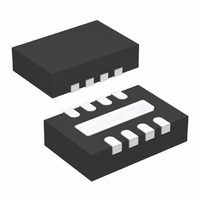
LTC4308IDD#PBF Linear Technology, LTC4308IDD#PBF Datasheet

LTC4308IDD#PBF
Specifications of LTC4308IDD#PBF
Available stocks
Related parts for LTC4308IDD#PBF
LTC4308IDD#PBF Summary of contents
Page 1
... L, LT, LTC and LTM are registered trademarks of Linear Technology Corporation. Hot Swap is a trademark of Linear Technology Corporation. All other trademarks are the property of their respective owners. Protected by U.S. Patents including 7032051, 6650174, 6356140. ...
Page 2
... EXPOSED PAD (PIN 9) CONNECTION TO GROUND IS OPTIONAL ORDER INFORMATION LEAD FREE FINISH TAPE AND REEL LTC4308CDD#PBF LTC4308CDD#TRPBF LTC4308IDD#PBF LTC4308IDD#TRPBF LTC4308CMS8#PBF LTC4308CMS8#TRPBF LTC4308IMS8#PBF LTC4308IMS8#TRPBF Consult LTC Marketing for parts specifi ed with wider operating temperature ranges. *Temperature grades are identifi label on the shipping container. ...
Page 3
ELECTRICAL CHARACTERISTICS temperature range, otherwise specifi cations are at T SYMBOL PARAMETER t Bus Idle Time IDLE V ENABLE Threshold Voltage THR_EN V ENABLE Threshold Voltage Hysteresis THR_EN(HYST) I ENABLE Input Current ENABLE t ENABLE Delay Off-On PLH_EN t ENABLE ...
Page 4
LTC4308 ELECTRICAL CHARACTERISTICS temperature range, otherwise specifi cations are at T SYMBOL PARAMETER Bus Stuck Low Timeout t Bus Stuck Low Timer TIMEOUT Timing Characteristics Maximum Operating Frequency I2C,MAX t Bus Free Time Between Stop and ...
Page 5
TYPICAL PERFORMANCE CHARACTERISTICS I Enabled Current CC vs Temperature 8.0 7 5.5V CC 7.0 6 3. 2.3V CC 5.5 5.0 4.5 4.0 –50 –25 0 TEMPERATURE (°C) Input-Output High to Low Propagation ...
Page 6
LTC4308 PIN FUNCTIONS ENABLE (Pin 1): Connection Enable Input. This 0.6V nomi- nal threshold input pin enables or disables the LTC4308. For normal operation, pull or connect ENABLE high. Driving ENABLE below the 0.45V threshold isolates SDAIN from SDAOUT, SCLIN ...
Page 7
BLOCK DIAGRAM Low Voltage Level Shifting 2-Wire Bus Buffer with Stuck Bus Recovery SDAIN 6 SCLIN 3 + – 0.6V + – 0.6V ENABLE + 1 – 0.6V CONNECT CONNECT PRECHARGE PC_CONNECT CONNECT CONNECT 30ms TIMER I BOOSTSCL I BOOSTSDA ...
Page 8
LTC4308 OPERATION Start-Up When the LTC4308 fi rst receives power on its V either during power-up or live insertion, it starts in an under voltage lockout (UVLO) state, ignoring any activity on the SDA or SCL pins until V rises ...
Page 9
OPERATION C = 50pF OUT 3.3V PULLUP(OUT 150pF IN V PULLUP(IN) 200ns/DIV Figure 2. Input-Output Rising Edge Waveforms Propagation Delays During a rising edge, the rise time on each side is infl u- ...
Page 10
LTC4308 OPERATION When powering up into a bus stuck low condition, the connection circuitry connecting the SDA and SCL pins are not activated. 30ms after UVLO, automatic clocking and stop bit generation takes place as described above. READY Digital Output ...
Page 11
APPLICATIONS INFORMATION Resistor Pull-Up Value Selection To guarantee the SDAOUT and SCLOUT rise time accelera- tors are activated during a rising edge, the bus must rise on its own with a positive slew rate of at least 0.8V/μs. To achieve ...
Page 12
LTC4308 APPLICATIONS INFORMATION Systems with Supply Voltage Droop In large 2-wire systems, the V voltages seen by devices CC at various points in the system can differ by a few hundred millivolts or more. This situation is modeled by a ...
Page 13
APPLICATIONS INFORMATION MIXED VOLTAGE BACKPLANE 3. 10k 10k SDA SCL READY ENA1 ENAn Figure 4. The LTC4308 in an Application with Staggered Connectors. MIXED VOLTAGE BACKPLANE 3. 10k 10k SDA SCL READY ENA1 ENAn ...
Page 14
LTC4308 TYPICAL APPLICATIONS V (BUS) SDA1 SCL1 READY 200Ω* TEMPERATURE SENSOR 200Ω* *200Ω ARE ADDITIONAL ESD PROTECTION RESISTORS CC(LTC4308) DROOP C1 0.01μ 10k 10k 10k V CC LTC4308 ENABLE SDAOUT SDAIN SCLOUT SCLIN READY ...
Page 15
... LEAD COPLANARITY (BOTTOM OF LEADS AFTER FORMING) SHALL BE 0.102mm (.004") MAX Information furnished by Linear Technology Corporation is believed to be accurate and reliable. However, no responsibility is assumed for its use. Linear Technology Corporation makes no represen- tation that the interconnection of its circuits as described herein will not infringe on existing patent rights. ...
Page 16
... High Defi nition Multimedia Interface (HDMI) Level Shifting 2-Wire Bus Buffer LTC4309 Level Shifting Low Offset Hot Swappable 2-Wire Bus Buffer with Stuck Bus Recovery ThinSOT is a trademark of Linear Technology Corporation 16 Linear Technology Corporation 1630 McCarthy Blvd., Milpitas, CA 95035-7417 (408) 432-1900 FAX: (408) 434-0507 ● ...


