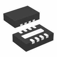
LTC4308IDD#PBF Linear Technology, LTC4308IDD#PBF Datasheet - Page 11

LTC4308IDD#PBF
Manufacturer Part Number
LTC4308IDD#PBF
Description
IC BUS BUFFER LV 8-DFN
Manufacturer
Linear Technology
Type
Hot-Swap Switchr
Datasheet
1.LTC4308CMS8PBF.pdf
(16 pages)
Specifications of LTC4308IDD#PBF
Applications
General Purpose, Buffer/Bus Extender
Internal Switch(s)
Yes
Voltage - Supply
2.3 V ~ 5.5 V
Operating Temperature
-40°C ~ 85°C
Mounting Type
Surface Mount
Package / Case
8-WFDFN Exposed Pad
Output Voltage
300mV
Internal Switch
No
Supply Voltage Range
2.3V To 5.5V
Digital Ic Case Style
DFN
No. Of Pins
8
Operating Temperature Range
-40°C To +85°C
Msl
MSL 1 - Unlimited
Interface
I2C
Rohs Compliant
Yes
Lead Free Status / RoHS Status
Lead free / RoHS Compliant
Available stocks
Company
Part Number
Manufacturer
Quantity
Price
APPLICATIONS INFORMATION
Resistor Pull-Up Value Selection
To guarantee the SDAOUT and SCLOUT rise time accelera-
tors are activated during a rising edge, the bus must rise
on its own with a positive slew rate of at least 0.8V/μs. To
achieve this, choose a maximum resistor value R
using the formula:
Where R
is the minimum bus pull-up supply voltage and C
the equivalent bus capacitance in pF .
To estimate the value of C
of capacitance per device on the bus (10pF for the device
and 10pF for interconnect).
In addition, R
the precharge voltage and provide logic highs on SDAOUT
and SCLOUT for the start-up and connection circuitry to
connect the backplane to the card. To meet this require-
ment, always choose
where V
Threshold Voltage, V
Further, on SDAIN and SCLIN and for heavily loaded
systems on SDAOUT and SCLOUT, where the selected
R
0.8V/μs, users must also guarantee
Live Insertion and Capacitance Buffering Application
Figure 4 and 5 illustrate applications of the LTC4308 that
take advantage of the LTC4308’s Hot Swap™, capacitance
buffering and output pin precharge features. If the I/O
cards were plugged directly into the backplane without the
LTC4308 buffer, all of the backplane and card capacitances
would add directly together, making rise time and fall time
PULLUP
R
R
R
PULLUP
PULLUP
PULLUP
THR(MAX)
PULLUP
value causes the bus to rise at a rate slower than
≤
≤ 75k
≤
PULLUP
(V
V
is the pull-up resistor value in kΩ, V
BUS(MIN)
BUS(MIN)
is the maximum specifi ed Logic Input
V
BUS(MIN)
must be strong enough to overcome
THR
V
100μA
THR(MAX)
.
− V
− 0.8V)• 1250ns / V
BUS
C
THR(MAX)
− V
BUS
, use a general rule of 20pF
THR(MAX)
− 1V
BUS(MIN)
PULLUP
BUS
is
requirements diffi cult to meet. Placing an LTC4308 on the
edge of each card isolates the card capacitance from the
backplane. For a given I/O card, the LTC4308 drives the
capacitance of everything on the card and the backplane
must drive only the capacitance of the LTC4308, which
is less than 10pF .
Figure 4 shows the LTC4308 used in the typical staggered
connector application, where V
“early power” pins. The “early power” pins ensure the
LTC4308 is initially powered and forcing the 1V precharge
voltage on the medium length SDA and SCL output pins
before they contact with the backplane busses. Coupled
with ENABLE as the shortest pin, passively pulled to ground
by a resistor, the staggered approach provides additional
time for transients associated with live insertion to settle
before the LTC4308 can be enabled.
Figure 5 shows the LTC4308 in an application where all
of the pins have the same length. In this application, a
resistor is used to hold the ENABLE pin low during live
insertion, until the backplane control circuitry can enable
the device.
Level Shifting Applications
Systems requiring different supply voltages for the
backplane side and the card side can use the LTC4308
for bidirectional level shifting, as shown in Figures 4, 5,
and 7. The LTC4308 can level shift between bus pull-up
supplies as low as 0.9V to as high as 5.5V. Level shifting
allows newer designs that require lower voltage supplies,
such as EEPROMs and microcontrollers, the capability to
interface with legacy backplanes which may be operating
at higher supply voltages.
The LTC4308’s negative offset voltage from output to
input allow level shifting applications with high SDAOUT
and SCLOUT V
SDAIN and SCLIN busses. Figure 7 shows an application
where 200Ω resistors, used to provide additional ESD
protection for the Temperature Sensor’s internal low
impedance pull-down device, generate high V
SDAOUT and SCLOUT busses.
OL
to effectively translate to the low voltage
CC
and GND are the longest
LTC4308
OL
11
on the
4308f


