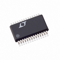
LTC4261IGN#PBF Linear Technology, LTC4261IGN#PBF Datasheet - Page 11

LTC4261IGN#PBF
Manufacturer Part Number
LTC4261IGN#PBF
Description
IC CTRLR HOTSWAP W/ADC 28-SSOP
Manufacturer
Linear Technology
Type
Hot-Swap Controllerr
Datasheet
1.LTC4261IGNPBF.pdf
(32 pages)
Specifications of LTC4261IGN#PBF
Applications
General Purpose
Internal Switch(s)
No
Voltage - Supply
9 V ~ 11.2 V
Operating Temperature
-40°C ~ 85°C
Mounting Type
Surface Mount
Package / Case
28-SSOP (0.150", 3.95mm Width)
Lead Free Status / RoHS Status
Lead free / RoHS Compliant
Available stocks
Company
Part Number
Manufacturer
Quantity
Price
The LTC4261/LTC4261-2 are designed to turn a board’s
supply voltage on and off in a controlled manner, allow-
ing the board to be safely inserted or removed from a
live – 48V backplane. The devices also feature an onboard
10-bit ADC and I
current, voltages and faults. The main functional circuits
of the LTC4261/LTC4261-2 are illustrated in the Block
Diagram.
In normal operation after a start-up debounce delay, the
GATE pin turns on the external N-channel FET passing
power to the load. The GATE pin is powered by a shunt
regulated 11.2V supply on the V
from –48V RTN through a dropping resistor. The turn-on
sequence starts by pulling the SS pin up. The voltage at
the SS pin is converted to a current, I
GATE up. When the pass FET starts to turn on and charge
the load capacitor, the inrush current fl owing through the
FET is a function of the capacitor at RAMP (C
capacitor (C
from the RAMP pin to C
I
SS pin voltage and are limited to 20µA and 11.5µA, respec-
tively when SS reaches its clamping voltage (2.56V).
The ACL amplifi er is used for overcurrent and short-circuit
protection. It monitors the load current through the SENSE
pin voltage and a sense resistor R
dition, the ACL amplifi er limits the current to 50mV/R
pulling down GATE in an active servo loop. After a 530µs
timeout, the ACL amplifi er turns off the pass FET. In the
event of a catastrophic short circuit, when V
150mV, a fast response comparator pulls the GATE pin
down with a 110mA current.
OPERATION
RAMP
I
INRUSH
and I
=
GATE(UP)
L
I
) and the ramp current (I
RAMP
2
C interface that allows monitoring board
•
are approximately proportional to the
C
C
R
L
R
:
S
. In an overcurrent con-
IN
GATE(UP)
pin that is derived
RAMP
SENSE
) that fl ows
, pulling the
R
), the load
crosses
S
by
The DRAIN and the GATE voltages are monitored to de-
termine if power is available for the load. Two power good
signals are sequenced on the PG pin (fi rst power good
signal) and the PGIO pin (second power good signal), each
with a debounce delay that is twice the start-up delay. The
PGIO pin can also be used as a general purpose input or
output. The PGI pin serves as a watchdog to monitor the
output of the DC/DC module. If the module output fails to
come up, the LTC4261/LTC4261-2 shut down.
The TMR pin generates delays for initial start-up, auto-retry
following a fault, power good outputs and PGI check.
The logic circuits a re powered by an internally generated
5V supply (available on the INTV
on the pass FET, both V
ceed their undervoltage lockout thresholds. In addition,
the control inputs UVH, UVL, OV, EN, ON and PGI are
monitored by comparators. The FET is held off until all
start-up conditions are met.
A 10-bit analog-to-digital converter (ADC) is included in the
LTC4261/LTC4261-2. The ADC measures SENSE resistor
voltage as well as voltage at the ADIN2/OV (SSOP/QFN) and
ADIN pins. The results are stored in on-board registers.
An I
It also allows the host to poll the device and determine if a
fault has occurred. If the ALERT line is used as an interrupt,
the host can respond to a fault in real time. The SDA line
is divided into SDAI (input) and SDAO (output) to facili-
tate opto coupling with the system host. Two three-state
pins, ADR0 and ADR1, are used to decode eight device
addresses. The interface can also be confi gured through
the ADR0 and ADR1 pins for a single-wire broadcast
mode, sending ADC data and faults status through the
SDAO pin to the host without clocking the SCL line. This
single-wire, one-way communication simplifi es system
design by eliminating two optocouplers on SCL and SDAI
that are required by an I
2
C interface is provided to read the ADC data registers.
LTC4261/LTC4261-2
IN
2
C interface.
and INTV
CC
pin). Prior to turning
CC
voltages must ex-
11
42612fb


