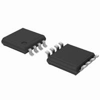
PCA9511ADP,118 NXP Semiconductors, PCA9511ADP,118 Datasheet - Page 4

PCA9511ADP,118
Manufacturer Part Number
PCA9511ADP,118
Description
IC HOTSWAP I2C/SMBUS BUFF 8TSSOP
Manufacturer
NXP Semiconductors
Type
I²C-Bus and SMBus Switchr
Datasheet
1.PCA9511ADP118.pdf
(24 pages)
Specifications of PCA9511ADP,118
Package / Case
8-TSSOP
Applications
Hot-Swap/SMB Buffer
Internal Switch(s)
Yes
Current Limit
50mA
Voltage - Supply
2.7 V ~ 5.5 V
Operating Temperature
-40°C ~ 85°C
Mounting Type
Surface Mount
Logic Family
PCA
Maximum Operating Temperature
85 C
Mounting Style
SMD/SMT
Minimum Operating Temperature
- 40 C
Number Of Lines (input / Output)
3 / 3
Propagation Delay Time
70 ns
Logic Type
Bus Buffer
Lead Free Status / RoHS Status
Lead free / RoHS Compliant
Lead Free Status / RoHS Status
Lead free / RoHS Compliant, Lead free / RoHS Compliant
Other names
568-3360-2
935279308118
PCA9511ADP-T
935279308118
PCA9511ADP-T
Available stocks
Company
Part Number
Manufacturer
Quantity
Price
Part Number:
PCA9511ADP,118
Manufacturer:
NXP/恩智浦
Quantity:
20 000
NXP Semiconductors
7. Pinning information
8. Functional description
PCA9511A_4
Product data sheet
7.1 Pinning
7.2 Pin description
8.1 Start-up
Table 3.
Refer to
An undervoltage/initialization circuit holds the parts in a disconnected state which
presents high-impedance to all SDA and SCL pins during power-up. A LOW on the
ENABLE pin also forces the parts into the low current disconnected state when the I
essentially zero. As the power supply is brought up and the ENABLE is HIGH or the part is
powered and the ENABLE is taken from LOW to HIGH it enters an initialization state
where the internal references are stabilized and the precharge circuit is enabled. At the
end of the initialization state the ‘Stop Bit And Bus Idle’ detect circuit is enabled. With the
ENABLE pin HIGH long enough to complete the initialization state (t
HIGH when all the SDA and SCL pins have been HIGH for the bus idle time or when all
pins are HIGH and a STOP condition is seen on the SDAIN and SCLIN pins, SDAIN is
connected to SDAOUT and SCLIN is connected to SCLOUT. The 1 V precharge circuitry
Symbol
ENABLE
SCLOUT
SCLIN
GND
READY
SDAIN
SDAOUT
V
Fig 2.
CC
SCLOUT
ENABLE
SCLIN
Figure 1 “Block diagram of
GND
Pin configuration for SO8
Pin description
Pin
1
2
3
4
5
6
7
8
1
2
3
4
PCA9511AD
Description
Chip enable. Grounding this input puts the part in a low current (< 1 A)
mode. It also disables the rise time accelerators, isolates SDAIN from
SDAOUT and isolates SCLIN from SCLOUT.
serial clock output to and from the SCL bus on the card
serial clock input to and from the SCL bus on the backplane
Ground. Connect this pin to a ground plane for best results.
open-drain output which pulls LOW when SDAIN and SCLIN are
disconnected from SDAOUT and SCLOUT, and goes HIGH when the two
sides are connected
serial data input to and from the SDA bus on the backplane
serial data output to and from the SDA bus on the card
power supply
002aab577
Rev. 04 — 19 August 2009
8
7
6
5
V
SDAOUT
SDAIN
READY
CC
PCA9511A”.
Hot swappable I
Fig 3.
SCLOUT
ENABLE
SCLIN
GND
Pin configuration for TSSOP8
2
1
2
3
4
C-bus and SMBus bus buffer
PCA9511ADP
PCA9511A
002aab578
en
) and remaining
© NXP B.V. 2009. All rights reserved.
8
7
6
5
V
SDAOUT
SDAIN
READY
CC
4 of 24
CC
is


