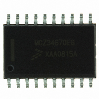
MCZ34670EGR2 Freescale Semiconductor, MCZ34670EGR2 Datasheet - Page 11

MCZ34670EGR2
Manufacturer Part Number
MCZ34670EGR2
Description
IC POE CURR MODE SW REG 20-SOIC
Manufacturer
Freescale Semiconductor
Type
Power Over Ethernet Controller (PoE)r
Datasheet
1.MCZ34670EGR2.pdf
(24 pages)
Specifications of MCZ34670EGR2
Applications
Remote Peripherals (Industrial Controls, Cameras, Data Access)
Internal Switch(s)
No
Voltage - Supply
60V
Operating Temperature
-40°C ~ 85°C
Mounting Type
Surface Mount
Package / Case
20-SOIC (0.300", 7.50mm Width)
Product
PoE / LAN Solutions
Supply Voltage (max)
80 V
Power Dissipation
800 mW
Operating Temperature Range
- 40 C to + 85 C
Mounting Style
SMD/SMT
Supply Current
4.5 mA
Output Current
2.1A
Digital Ic Case Style
SOIC
No. Of Pins
20
Duty Cycle (%)
48%
Uvlo
2V
Frequency
400kHz
Msl
MSL 3 - 168 Hours
Rohs Compliant
Yes
Lead Free Status / RoHS Status
Lead free / RoHS Compliant
Other names
MCZ34670EGR2
MCZ34670EGR2TR
MCZ34670EGR2TR
Available stocks
Company
Part Number
Manufacturer
Quantity
Price
Company:
Part Number:
MCZ34670EGR2
Manufacturer:
KODENSHI
Quantity:
6 400
802.3af Powered Devices (PD) and a high performance
current mode switching regulator. It allows a designer to build
PDs with a minimum of external components by means of
integrating the required IEEE 802.3af functions and all
functions necessary to build a high efficiency DC/DC
converter. Thus 34670 gives the system designer a device
that drastically reduces cost and board space.
standard and provides complete signature detection and
power classification functions. It controls inrush current
limiting and incorporates an adjustable undervoltage lockout.
The 34670 includes thermal protection circuitry to protect the
device in case of high power dissipation.
POSITIVE SUPPLY VOLTAGE INPUT (VPWR)
connects between this pin and the V
CLASSIFICATION RESISTOR (RCLA)
class of the PD.
UNDERVOLTAGE LOOKOUT (UVLO)
connected to V
TEST PINS (TEST1, TEST2)
FREQUENCY ADJUSTMENT (FREQ)
resistor between FREQ and V
INRUSH CURRENT LIMIT (ILIM)
switch, add a resistor between ILIM and V
NEGATIVE SUPPLY VOLTAGE (VIN)
OUTPUT VOLTAGE (VOUT)
current path and low current path).
Analog Integrated Circuit Device Data
Freescale Semiconductor
The 34670 combines a Power Interface Port for IEEE
On the PD side the 34670 fully supports the IEEE802.3af
This is the most positive power supply input. The load
Connect a resistor between RCLA and V
Used to adjust the undervoltage lookout threshold voltage,
Connect to V
Adjusts the internal oscillator frequency by connecting a
Used to adjust the inrush current limit of the isolation
This is the most negative power supply input.
This pin is the drain of the internal Power MOSFET (high
IN
IN
to use the default threshold voltage.
in application mode.
IN
.
OUT
pin.
IN
FUNCTIONAL DESCRIPTION
IN
.
FUNCTIONAL PIN DESCRIPTION
to select the
INTRODUCTION
protect the external switching MOSFET by disabling the gate
driver in case of input line overvoltage.
regulation. It drives an external power MOSFET with sense
resistor. The switching frequency is adjustable between
100 kHz and 400 kHz. The output voltage feedback
information can be accomplished by an optocoupler, if
isolation is required.
signature detection, classification and proper turn on and turn
off of the DC/DC converter.
RESET OUTPUT (RESET)
referenced to V
SOFT START INPUT (SS)
source charges the capacitor and generates a soft-start
ramp.
COMPENSATION PIN (COMP)
for feedback compensation. COMP is pulled-up by an
internal 5.0 kΩ resistor to 5.0 V.
FEEDBACK INPUT (FB)
isolated applications it’s connected to the secondary output
through a resistor divider.
CURRENT SENSE (CS)
proportional to the current through the sense resistor.
GATE DRIVER OUTPUT (GATE)
GATE sources and sinks up to 1.0 A.
VDD OUTPUT (VDD)
MOSFET. Connect a capacitor from V
The 34670 also offers an input overvoltage detection to
The switching regulator provides excellent line and load
An internal logic control block manages the sequencing of
This is an active-low RESET output signal. This pin is
Connect an external capacitor to SS. The internal current
COMP is the output of the error amplifier and is available
This is the inverting input of the error amplifier. In non-
The current sense pin CS senses a voltage that is
GATE drives the gate of the external power MOSFET.
V
DD
mainly supplies the gate of the external power
OUT
.
FUNCTIONAL DESCRIPTION
DD
to V
INTRODUCTION
OUT
.
34670
11


