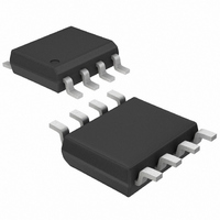
MAX4271ESA+ Maxim Integrated Products, MAX4271ESA+ Datasheet - Page 15

MAX4271ESA+
Manufacturer Part Number
MAX4271ESA+
Description
IC CNTRLR HOT SWAP 8-SOIC
Manufacturer
Maxim Integrated Products
Type
Hot-Swap Controllerr
Datasheet
1.MAX4271ESA.pdf
(26 pages)
Specifications of MAX4271ESA+
Applications
General Purpose
Internal Switch(s)
No
Voltage - Supply
2.7 V ~ 13.2 V
Operating Temperature
-40°C ~ 85°C
Mounting Type
Surface Mount
Package / Case
8-SOIC (0.154", 3.90mm Width)
Product
Controllers & Switches
Supply Voltage (max)
13.2 V
Supply Voltage (min)
2.7 V
Power Dissipation
471 mW
Operating Temperature Range
- 40 C to + 85 C
Mounting Style
SMD/SMT
Lead Free Status / RoHS Status
Lead free / RoHS Compliant
is stable. Any input voltage transient at IN below the
UVLO threshold will reset the device and initiate a start-
up sequence.
These devices also have an overvoltage lockout
(OVLO) feature that prevents the device from restarting
after a fault condition if the discharge has not been
completed. V
Additionally, the MAX4273 LLMON pin discharges the
load line with a 1kΩ pulldown and prevents startup until
the load voltage is below 0.1V.
Since the MAX4271/MAX4272 do not monitor the output
voltage, a startup sequence can be initiated while the
board capacitance is still charged.
A large board capacitance or a short startup period may
prevent the MAX4272 from charging completely in one
startup period. The MAX4272 responds to these condi-
tions by charging the capacitor with bursts defined by a
t
ing will be complete after several retries unless the resis-
tive load or current load excessively discharges the
board capacitance during the retry timeout. This feature
applies to the MAX4273 if LLMON is left floating or is
connected to GND. To prevent multiple charging bursts,
ensure that the t
required to complete the charge of the board capaci-
tance (see Component Selection).
New-generation MOSFETs have an absolute maximum
rating of ±8V for the gate-to-source voltage (V
protect these MOSFETs, the MAX4271/MAX4272 limit the
gate-to-drain voltage (the MAX4273 limits the gate-to-
source voltage) to +7.5V with an internal zener diode. No
protection is provided for negative V
MAX4272). If GATE can be discharged to ground faster
than the output voltage, an external small-signal protec-
tion diode (D1) can be used, as shown in Figure 6. The
MAX4273 has the protection diode internal.
Figure 5. Status (STAT) Output Timing Diagram
ON
with Autoretry, DualSpeed/BiLevel Fault Protection
(CTON)*
*MAX4273 ONLY
CTIM
STAT
duty cycle and a period of t
ON
3V to 12V Current-Limiting Hot-Swap Controllers
1.2V
V
V
IN
IN
O
O
O
GATE
ON
______________________________________________________________________________________
Gate Overvoltage Protection
has to be discharged to below 0.1V.
t
START
timer exceeds the minimum time
ON
NO FAULT CONDITIONS PRESENT
+ t
RETRY
GS
. The charg-
(MAX4271/
FAULT CONDITION,
OR ON FALLING
EDGE
GS
). To
Select the external N-channel MOSFET according to
the application’s current level. Table 2 lists some rec-
ommended components. The MOSFET’s on-resistance
(R
imum voltage drop at full load to limit the MOSFET
power dissipation. High R
ple if the board has pulsing loads or triggers an exter-
nal undervoltage reset monitor at full load. Determine
the device power-rating requirement to accommodate
a short circuit on the board at startup with the device
Figure 6. External Gate-Source Protection
Table 2. Recommended N-Channel
MOSFETs
IRF7413
IRF7401
IRL3502S
MMSF3300
MMSF5N02H
MTB60N05H
FDS6670A
NDS8426A
FDB8030L
DS(ON)
NUMBER
PART
) should be chosen low enough to have a min-
CHARGE PUMP
GATE DRIVE
MAX4271
MAX4272
Applications Information
MANUFACTURER
International
Fairchild
Motorola
Rectifier
DS(ON)
Component Selection
IN
SENSE
GATE
V
GD
can cause output rip-
V
N-Channel MOSFET
GS
D1
11mΩ, 8 SO, 30V
22mΩ, 8 SO, 20V
6mΩ, D2PAK, 20V
20mΩ, 8 SO, 30V
30mΩ, 8 SO, 20V
14mΩ, D2PAK, 50V
10mΩ, 8 SO, 30V
13.5mΩ, 8 SO, 20V
4.5mΩ, D2PAK, 30V
DESCRIPTION
M1
N
V
R
OUT
C
SENSE
BOARD
15


