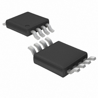
LTC4301CMS8 Linear Technology, LTC4301CMS8 Datasheet - Page 6

LTC4301CMS8
Manufacturer Part Number
LTC4301CMS8
Description
IC BUFFER BUS HOTSWAP 2WR 8MSOP
Manufacturer
Linear Technology
Type
Hot-Swap Switchr
Datasheet
1.LTC4301CMS8PBF.pdf
(12 pages)
Specifications of LTC4301CMS8
Applications
General Purpose, Buffer/Bus Extender
Internal Switch(s)
Yes
Voltage - Supply
2.7 V ~ 5.5 V
Operating Temperature
0°C ~ 70°C
Mounting Type
Surface Mount
Package / Case
8-TSSOP, 8-MSOP (0.118", 3.00mm Width)
Lead Free Status / RoHS Status
Contains lead / RoHS non-compliant
Available stocks
Company
Part Number
Manufacturer
Quantity
Price
Company:
Part Number:
LTC4301CMS8
Manufacturer:
LT
Quantity:
10 000
Part Number:
LTC4301CMS8#PBF
Manufacturer:
LINEAR/凌特
Quantity:
20 000
Company:
Part Number:
LTC4301CMS8#TRPBF
Manufacturer:
MAXIM
Quantity:
6 220
Part Number:
LTC4301CMS8#TRPBF
Manufacturer:
LINEAR/凌特
Quantity:
20 000
OPERATIO
LTC4301
There is a finite high to low propagation delay through the
connection circuitry for falling waveforms. Figure 2 shows
the falling edge waveforms for the same pull-up resistors
and equivalent capacitance conditions as used in Figure 1.
An external N-channel MOSFET device pulls down the
voltage on the side with 55pF capacitance; LTC4301 pulls
down the voltage on the opposite side with a delay of 60ns.
This delay is always positive and is a function of supply
voltage, temperature and the pull-up resistors and equiva-
lent bus capacitances on both sides of the bus. The Typical
Performance Characteristics section shows high to low
propagation delay as a function of temperature and volt-
age for 10k pull-up resistors pulled-up to V
equivalent capacitance on both sides of the part. Larger
output capacitances translate to longer delays (up to
150ns). Users must quantify the difference in propagation
times for a rising edge versus a falling edge in their
systems and adjust setup and hold times accordingly.
6
INPUT
1V/DIV
SIDE
55pF
Figure 2. Input-Output Connection
High to Low Propagation Delay
U
20ns/DIV
4301 F02
CC
OUTPUT
SIDE
20pF
and 100pF
Ready Digital Output
This pin provides a digital flag which is low when either CS
is high or the start-up sequence described earlier in this
section has not been completed. READY goes high when
CS is low and start-up is complete. The pin is driven by an
open-drain pull-down capable of sinking 3mA while hold-
ing 0.4V on the pin. Connect a resistor of 10k to V
provide the pull-up.
Connection Sense
When the CS pin is driven above 1.4V with respect to the
LTC4301’s ground, the backplane side is disconnected
from the card side and the READY pin is internally pulled
low. When the pin voltage is low, the part waits for data
transactions on both the backplane and card sides to be
complete (as described in the Start-Up section) before
reconnecting the two sides. At this time the internal
pulldown on READY releases.
CC
4301fb
to


