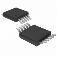
LTC4214-2CMS#TRPBF Linear Technology, LTC4214-2CMS#TRPBF Datasheet - Page 8

LTC4214-2CMS#TRPBF
Manufacturer Part Number
LTC4214-2CMS#TRPBF
Description
IC CTRLR HOTSWAP NEGVOLT 10MSOP
Manufacturer
Linear Technology
Type
Hot-Swap Controllerr
Datasheet
1.LTC4214-1CMS.pdf
(32 pages)
Specifications of LTC4214-2CMS#TRPBF
Applications
General Purpose
Internal Switch(s)
No
Voltage - Supply
6 V ~ 16 V
Operating Temperature
0°C ~ 70°C
Mounting Type
Surface Mount
Package / Case
10-TFSOP, 10-MSOP (0.118", 3.00mm Width)
Linear Misc Type
Negative Low Voltage
Family Name
LTC4214-2
Package Type
MSOP
Operating Supply Voltage (min)
-6V
Operating Supply Voltage (max)
-16V
Operating Temperature (min)
0C
Operating Temperature (max)
70C
Operating Temperature Classification
Commercial
Product Depth (mm)
3mm
Product Height (mm)
0.86mm
Product Length (mm)
3mm
Mounting
Surface Mount
Pin Count
10
Lead Free Status / RoHS Status
Lead free / RoHS Compliant
Available stocks
Company
Part Number
Manufacturer
Quantity
Price
PI FU CTIO S
LTC4214-1/LTC4214-2
V
positive side of the supply via a resistor. An internal
undervoltage lockout (UVLO) circuit holds GATE low until
the V
OV. If UV is high, OV is low and V
TIMER starts an initial timing cycle before initiating a GATE
ramp-up. If V
pulls low immediately.
PWRGD (Pin 2): Power Good Status Output. At start-up,
PWRGD latches low if DRAIN is below 1.232V and GATE
is within 2.8V of V
(UVLO) or a circuit breaker fault timeout. This pin is
internally pulled high by a 50 A current source.
SS (Pin 3): Soft-Start Pin. This pin is used to ramp inrush
current during start up, thereby effecting control over di/
dt. A 20x attenuated version of the SS pin voltage is
presented to the current limit amplifier. This attenuated
voltage limits the MOSFET’s drain current through the
sense resistor during the soft-start current limiting. At the
beginning of a start-up cycle, the SS capacitor (C
ramped by a 22 A current source. The GATE pin is held
low until SS exceeds 20 • V
shunted by a 73k resistor (R
voltage to 1.6V. This corresponds to an analog current
limit SENSE voltage of 70mV. If the SS capacitor is
omitted, the SS pin ramps from 0V to 1.6V in about 220 s.
The SS pin is pulled low under any of the following
conditions: in UVLO, in an undervoltage condition, in an
overvoltage condition, during the initial timing cycle or
when the circuit breaker fault times out.
SENSE (Pin 4): Circuit Breaker/Current Limit Sense Pin.
Load current is monitored by a sense resistor R
nected between SENSE and V
steps. If SENSE exceeds V
comparator activates a (40 A + 8 • I
current. If SENSE exceeds V
rent limit amplifier pulls GATE down to regulate the MOSFET
current at V
circuit, SENSE may overshoot 70mV. If SENSE reaches
8
IN
U
(Pin 1): Positive Supply Input. Connect this pin to the
IN
pin is greater than V
U
ACL
IN
/R
drops below approximately 4.8V, GATE
S
IN
. In the event of a catastrophic short-
. PWRGD status is reset by UV, V
U
CB
LKO
ACL
OS
(50mV), the circuit breaker
SS
EE
(5.1V), overriding UV and
) which limits the SS pin
, and controlled in three
(70mV), the analog cur-
= 0.2V. SS is internally
IN
comes out of UVLO,
DRN
) TIMER pull-up
S
SS
con-
) is
IN
V
GATE low with a strong pull-down. To disable the circuit
breaker and current limit functions, connect SENSE to V
V
pin to the negative side of the power supply.
GATE (Pin 6): N-Channel MOSFET Gate Drive Output. This
pin is pulled high by a 50 A current source. GATE is pulled
low by invalid conditions at V
breaker fault timeout. GATE is actively servoed to control
the fault current as measured at SENSE. A compensation
capacitor at GATE stabilizes this loop. A comparator
monitors GATE to ensure that it is low before allowing an
initial timing cycle, GATE ramp-up after an overvoltage
event or restart after a current limit fault. During GATE
start-up, a second comparator detects if GATE is within
2.8V of V
DRAIN (Pin 7): Drain Sense Input. DRAIN measures the
drain-source voltage of the external N-channel MOSFET
switch for two purposes: first, a comparator detects when
V
tor, controls the status of the PWRGD output. Second, if
V
4.2V (V
plied by 8 and added to the TIMER’s 40 A pull-up current
during a circuit breaker fault cycle. This reduces the
fault time and MOSFET heating under conditions of high
dissipation.
OV (Pin 8): Overvoltage Input. The active high threshold at
the OV pin is set at 3V with respect to V
0.15V hysteresis. If OV > 3V, GATE pulls low. When OV
returns below 2.85V, GATE start-up begins without an
initial timing cycle. If an overvoltage condition occurs in
the middle of an initial timing cycle, the initial timing cycle
is restarted after the overvoltage condition goes away. An
overvoltage condition does not reset the PWRGD flag. The
internal UVLO at V
capacitor at OV prevents transients and switching noise
from affecting the OV thresholds and prevents glitches at
the GATE pin.
FCL
EE
DS
DS
(Pin 5): Negative Supply Voltage Input. Connect this
< 1.232V and together with the GATE high compara-
is greater than the DRAIN clamp of approximately
(200mV), the fast current limit comparator pulls
DRNCL
IN
before PWRGD is set.
), the current through resistor R
IN
always overrides OV. A 1nF to 10nF
IN
(UVLO), UV, OV, or a circuit
EE
and exhibits
D
is multi-
421412f
EE
.


