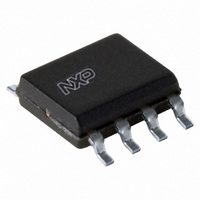
PCA9514AD,118 NXP Semiconductors, PCA9514AD,118 Datasheet - Page 15

PCA9514AD,118
Manufacturer Part Number
PCA9514AD,118
Description
IC I2C/SMBUS BUFF 8SOIC
Manufacturer
NXP Semiconductors
Type
I²C-Bus and SMBus Switchr
Datasheet
1.PCA9514ADP118.pdf
(26 pages)
Specifications of PCA9514AD,118
Package / Case
8-SOIC (0.154", 3.90mm Width)
Applications
Hot-Swap/SMB Buffer
Internal Switch(s)
Yes
Current Limit
50mA
Voltage - Supply
2.7 V ~ 5.5 V
Operating Temperature
-40°C ~ 85°C
Mounting Type
Surface Mount
Logic Family
PCA
Supply Voltage (max)
7 V
Supply Voltage (min)
- 0.5 V
Maximum Operating Temperature
+ 85 C
Mounting Style
SMD/SMT
Minimum Operating Temperature
- 40 C
Output Voltage
0.3 V
Propagation Delay Time
80 ns
Supply Current
3.5 mA
Logic Type
SMBus Bus Buffer
Lead Free Status / RoHS Status
Lead free / RoHS Compliant
Lead Free Status / RoHS Status
Lead free / RoHS Compliant, Lead free / RoHS Compliant
Other names
935279867118
PCA9514AD-T
PCA9514AD-T
PCA9514AD-T
PCA9514AD-T
NXP Semiconductors
Table 5.
V
[1]
[2]
PCA9513A_PCA9514A_4
Product data sheet
Symbol
Rise time accelerators
I
Input-output connection
V
t
t
C
V
I
I
I
System characteristics
f
t
t
t
t
t
t
t
t
t
t
trt(pu)
PLH
PHL
pu(SCLIN)
pu(SDAIN)
LI
SCL
BUF
HD;STA
SU;STA
SU;STO
HD;DAT
SU;DAT
LOW
HIGH
f
r
CC
offset
OL
i(SCL/SDA)
= 2.7 V to 5.5 V; T
This specification applies over the full operating temperature range.
The enable time can slow considerably for some parts when temperature is < 20 C.
Characteristics
Parameter
transient boosted pull-up
current
offset voltage
LOW to HIGH propagation
delay
HIGH to LOW propagation
delay
SCL and SDA input
capacitance
LOW-level output voltage
pull-up current on pin SCLIN
pull-up current on pin SDAIN
input leakage current
SCL clock frequency
bus free time between a
STOP and START condition
hold time (repeated) START
condition
set-up time for a repeated
START condition
set-up time for STOP
condition
data hold time
data set-up time
LOW period of the SCL clock
HIGH period of the SCL clock
fall time of both SDA and SCL
signals
rise time of both SDA and
SCL signals
amb
= 40 C to +85 C; unless otherwise specified.
…continued
Conditions
positive transition on
SDA, SCL; V
slew rate = 1.25 V/ s
10 k to V
SCL; V
SCL to SCL and
SDA to SDA;
10 k to V
C
SCL to SCL and
SDA to SDA;
10 k to V
C
V
pins; I
V
V
PCA9513A only
V
PCA9513A only
SDAn, SCLn pins;
V
I
CC
ENABLE
ENABLE
CC
L
L
= 0 V; SDAn, SCLn
= 100 pF each side
= 100 pF each side
Rev. 04 — 18 August 2009
= 2.7 V
= 5.5 V
sink
CC
= V
= V
= 3 mA;
= 3.3 V
CC
CC
CC
CC
CC
CC
;
;
on SDA,
;
;
= 2.7 V;
Hot swappable I
PCA9513A; PCA9514A
[1][7][9]
[5][6]
[4][8]
[4][8]
[4]
[1]
[9]
[9]
[4]
[4]
[4]
[4]
[4]
[4]
[4]
[4]
[4]
Min
1
0
-
-
-
0
65
65
0
1.3
0.6
0.6
0.6
300
100
1.3
0.6
20 + 0.1
20 + 0.1
1
2
C-bus and SMBus bus buffer
C
C
b
b
Typ
2
118
20
80
6
0.3
112
112
-
-
-
-
-
-
-
-
-
-
-
-
© NXP B.V. 2009. All rights reserved.
Max
-
175
-
-
8
0.4
150
150
+1
400
-
-
-
-
-
-
-
-
300
300
15 of 26
Unit
mA
mV
ns
ns
pF
V
kHz
ns
ns
ns
ns
A
A
A
s
s
s
s
s
s


