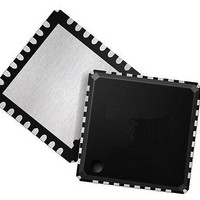
MAX3799ETJ+ Maxim Integrated Products, MAX3799ETJ+ Datasheet - Page 17

MAX3799ETJ+
Manufacturer Part Number
MAX3799ETJ+
Description
IC LIMITING AMP/VCSEL DVR 32TQFN
Manufacturer
Maxim Integrated Products
Type
Laser Diode Driverr
Datasheet
1.MAX3799ETJ.pdf
(36 pages)
Specifications of MAX3799ETJ+
Data Rate
14Gbps
Number Of Channels
1
Voltage - Supply
2.85 V ~ 3.63 V
Current - Supply
97mA
Current - Modulation
12mA
Current - Bias
15mA
Operating Temperature
-40°C ~ 85°C
Package / Case
32-WFQFN Exposed Pad
Mounting Type
Surface Mount
Input Voltage Range (max)
4 V
Operating Supply Voltage
2.85 V to 3.63 V
Supply Current
97 mA
Operating Temperature Range
- 40 C to + 85 C
Bandwidth
400 KHz to 1000 KHz
Mounting Style
SMD/SMT
Power Dissipation
2759 mW
Lead Free Status / RoHS Status
Lead free / RoHS Compliant
The bias current from the MAX3799 is optimized to pro-
vide up to 15mA of bias current into a 50Ω to 75Ω
VCSEL load with 40μA resolution. The bias current is
controlled through the 3-wire digital interface using the
SET_IBIAS, IBIASMAX, and BIASINC registers.
For VCSEL operation, the IBIASMAX register is first pro-
grammed to a desired maximum bias current value (up
to 15mA). The bias current to the VCSEL then can
range from zero to the value programmed into the
IBIASMAX register. The bias current level is stored in
the 9-bit SET_IBIAS register. Only bits 1 to 8 are written
to. The LSB (bit 0) of SET_IBIAS is initialized to zero
and is updated through the BIASINC register.
The value of the SET_IBIAS DAC register is updated
when the BIASINC register is addressed through the
3-wire interface. The BIASINC register is an 8-bit regis-
ter where the first 5 bits contain the increment informa-
tion in two’s complement notation. Increment values
range from -8 to +7 LSBs. If the updated value of
SET_IBIAS[8:1] exceeds IBIASMAX[7:0], the IBIASERR
warning flag is set and SET_IBIAS[8:0] remains
unchanged.
The modulation current from the MAX3799 is optimized
to provide up to 12mA of modulation current into a
100Ω differential load with 40μA resolution. The modu-
lation current is controlled through the 3-wire digital
interface using the SET_IMOD, IMODMAX, MODINC,
and SET_TXDE registers.
For VCSEL operation, the IMODMAX register is first pro-
grammed to a desired maximum modulation current
value (up to 12mA into a 100Ω differential load). The
modulation current to the VCSEL then can range from
zero to the value programmed into the IMODMAX regis-
ter. The modulation current level is stored in the 9-bit
SET_IMOD register. Only bits 1 to 8 are written to. The
LSB (bit 0) of SET_IMOD is initialized to zero and is
updated through the MODINC register.
The value of the SET_IMOD DAC register is updated
when the MODINC register is addressed through the
3-wire interface. The MODINC register is an 8-bit regis-
ter where the first 5 bits contain the increment informa-
tion in two’s complement notation. Increment values
range from -8 to +7 LSBs. If the updated value of
1Gbps to 14Gbps, SFP+ Multirate Limiting
______________________________________________________________________________________
Modulation Current DAC
Bias Current DAC
Amplifier and VCSEL Driver
SET_IMOD[8:1] exceeds IMODMAX[7:0], the IMODERR
warning flag is set and SET_IMOD[8:0] remains
unchanged.
The output driver is optimized for an AC-coupled 100Ω
differential load. The output stage also features program-
mable deemphasis that allows the deemphasis ampli-
tude to be set as a percentage of the modulation current.
The deemphasis function is enabled by the TXDE_EN
bit. At initial setup, the required amount of deemphasis
can be set using the SET_TXDE register. During the
system operation, it is advised to use the incremental
mode that updates the deemphasis (SET_TXDE) and
the modulation current DAC (SET_IMOD) simultaneous-
ly through the MODINC register.
Power-on reset ensures that the laser is off until the
supply voltage has reached a specified threshold
(2.55V). After power-on reset, bias current and modula-
tion current ramp up slowly to avoid an overshoot. In
the case of a POR, all registers are reset to their default
values.
Current out of the BMON pin is typically 1/16th the
value of I
voltage gain. An internal comparator latches a SOFT
FAULT if the voltage on BMON exceeds the value of
V
The safety and output control circuitry contains a dis-
able pin (DISABLE) and disable bit (TX_EN), along with
a FAULT indicator and fault detectors (Figure 3). The
MAX3799 has two types of faults, HARD FAULT and
SOFT FAULT. A HARD FAULT triggers the FAULT pin
and the output to the VCSEL is disabled. A SOFT
FAULT operates more like a warning and the outputs
are not disabled. Both types of faults are stored in the
TXSTAT1 and TXSTAT2 registers.
The FAULT pin is a latched output that can be cleared
by toggling the DISABLE pin. Toggling the DISABLE
pin also clears the TXSTAT1 and TXSTAT2 registers. A
single-point fault can be a short to V
3 shows the circuit response to various single-point
failures.
CC
- 0.55V.
BIAS
Eye Safety and Output Control Circuitry
. A resistor to ground at BMON sets the
Power-On Reset (POR)
Bias Current Monitor
CC
or GND. Table
Output Driver
17


