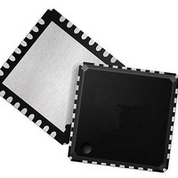
MAX3799ETJ+ Maxim Integrated Products, MAX3799ETJ+ Datasheet - Page 5

MAX3799ETJ+
Manufacturer Part Number
MAX3799ETJ+
Description
IC LIMITING AMP/VCSEL DVR 32TQFN
Manufacturer
Maxim Integrated Products
Type
Laser Diode Driverr
Datasheet
1.MAX3799ETJ.pdf
(36 pages)
Specifications of MAX3799ETJ+
Data Rate
14Gbps
Number Of Channels
1
Voltage - Supply
2.85 V ~ 3.63 V
Current - Supply
97mA
Current - Modulation
12mA
Current - Bias
15mA
Operating Temperature
-40°C ~ 85°C
Package / Case
32-WFQFN Exposed Pad
Mounting Type
Surface Mount
Input Voltage Range (max)
4 V
Operating Supply Voltage
2.85 V to 3.63 V
Supply Current
97 mA
Operating Temperature Range
- 40 C to + 85 C
Bandwidth
400 KHz to 1000 KHz
Mounting Style
SMD/SMT
Power Dissipation
2759 mW
Lead Free Status / RoHS Status
Lead free / RoHS Compliant
ELECTRICAL CHARACTERISTICS (continued)
(V
put load is AC-coupled to differential 100Ω (see Figure 1), typical values are at +25°C, V
otherwise specified. Registers are set to default values unless otherwise noted, and the 3-wire interface is static during measure-
ments. For testing, the RATE_SEL bit was used and the RSEL pin was left open.)
BIAS Current DAC Stability
Compliance Voltage at BIAS
BIAS Current Monitor Current
Gain
Compliance Voltage at BMON
BIAS Current Monitor Current
Gain Stability
Tx SAFETY FEATURES
Excessive Voltage at BMON
Excessive Voltage at BIAS
Maximum VCSEL Current in Off
State
SFP TIMING REQUIREMENTS
DISABLE Assert Time
DISABLE Negate Time
FAULT Reset Time of Power-On
Time
FAULT Reset Time
DISABLE to Reset
OUTPUT_LEVEL VOLTAGE DAC (SET_CML)
Full-Scale Voltage
Resolution
Integral Nonlinearity
LOS THRESHOLD VOLTAGE DAC (SET_LOS)
Full-Scale Voltage
Resolution
Integral Nonlinearity
BIAS CURRENT DAC (SET_IBIAS)
Full-Scale Current
CC
= 2.85V to 3.63V, T
PARAMETER
1Gbps to 14Gbps, SFP+ Multirate Limiting
_______________________________________________________________________________________
A
= -40°C to +85°C, CML receiver output load is AC-coupled to differential 100Ω, C
SYMBOL
t_
V
V
I
I
V
V
t_
t_
BMON
BMON
t_
BMON
BMON
I
FAULT
V
V
INL
INL
BIAS
BIAS
OFF
I
OFF
INIT
FS
ON
FS
FS
2mA
External resistor to GND defines the
voltage gain
2mA
Average voltage, FAULT warning always
occurs for V
warning never occurs for V
0.65V
Average voltage, FAULT always occurs for
V
V
FAULT or DISABLE, V
Time from rising edge of DISABLE input
signal to I
I
Time from falling edge of DISABLE to I
and I
FAULT = 0 before reset
Time from power-on or negation of FAULT
using DISABLE
Time from fault to FAULT on,
C
Time DISABLE must be held high to reset
FAULT
100 differential resistive load
5mA
11mV
MODOFF
BIAS
BIAS
FAULT
MOD
P-P
I
I
I
Amplifier and VCSEL Driver
BIAS
BIAS
CML_LEVEL
0.44V, FAULT never occurs for
0.65V
20pF, R
BIAS
at 90% of steady state when
V
BMON
TH_LOS
15mA (Notes 2, 10)
15mA (Note 10)
CONDITIONS
= I
FAULT
BIASOFF
V
20mA
CC
BIAS
94mV
= 4.7k
- 0.55V, FAULT
and I
BMON
= V
P-P
CC
MOD
V
CC
=
CC
BIAS
-
= 3.3V, I
0.65V
V
0.44
MIN
0.9
CC
0
5
BIAS
-
= 6mA, I
V
1200
±0.7
TYP
0.6V
0.48
±0.9
1.5
16
CC
94
21
AZ
5
-
= 1nF, transmitter out-
MOD
0.55V
V
MAX
0.65
500
100
2.1
1.8
CC
25
10
4
5
1
= 6mA, unless
-
UNITS
mV
mV
mV
mV
mA/A
LSB
LSB
mA
ms
μA
μs
μs
μs
μs
%
%
V
V
V
V
P-P
P-P
P-P
P-P
5


