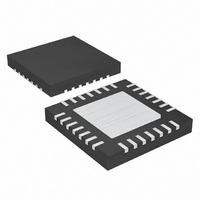
DS1864T+ Maxim Integrated Products, DS1864T+ Datasheet - Page 68

DS1864T+
Manufacturer Part Number
DS1864T+
Description
IC LASER CTRLR 1CHAN 5.5V 28TQFN
Manufacturer
Maxim Integrated Products
Type
Laser Diode Controller (Fiber Optic)r
Datasheet
1.DS1864TTR.pdf
(72 pages)
Specifications of DS1864T+
Number Of Channels
1
Voltage - Supply
2.97 V ~ 5.5 V
Current - Supply
3mA
Operating Temperature
-40°C ~ 95°C
Package / Case
28-WFQFN Exposed Pad
Mounting Type
Surface Mount
Lead Free Status / RoHS Status
Lead free / RoHS Compliant
SFP Laser Controller and
Diagnostic IC
The following terminology is commonly used to describe
I
Master Device: The master device controls the slave
devices on the bus. The master device generates SCL
clock pulses, and start and stop conditions.
Slave Devices: Slave devices send and receive data
at the master’s request.
Bus Idle or Not Busy: Time between stop and start
conditions when both SDA and SCL are inactive and in
their logic-high states. When the bus is idle, it often initi-
ates a low-power (or idle) mode for slave devices.
Start Condition: A start condition is generated by the
master to initiate a new data transfer with a slave.
Transitioning SDA from high to low while SCL remains
high generates a start condition. See the Timing
Diagrams for applicable timing.
Stop Condition: A stop condition is generated by the
master to end a data transfer with a slave. Transitioning
SDA from low to high while SCL remains high gener-
ates a stop condition. See the Timing Diagrams for
applicable timing.
Repeated Start Condition: The master can use a repeat-
ed start condition at the end of one data transfer to indi-
cate that it will immediately initiate a new data transfer
following the current one. Repeated starts are commonly
used during read operations to identify a specific memory
address to begin a data transfer. A repeated start condi-
tion is issued identically to a normal start condition. See
the Timing Diagrams for applicable timing.
Bit Write: Transitions of SDA must occur during the low
state of SCL. The data on SDA must remain valid and
unchanged during the entire high pulse of SCL plus the
setup and hold time requirements (Figure 19). Data is
shifted into the device during the rising edge of the SCL.
Bit Read: At the end a write operation, the master must
release the SDA bus line for the proper amount of setup
time (Figure 19) before the next rising edge of SCL during
a bit read. The device shifts out each bit of data on SDA
at the falling edge of the previous SCL pulse and the data
bit is valid at the rising edge of the current SCL pulse.
Remember that the master generates all SCL clock puls-
es, including when it is reading bits from the slave.
Acknowledgement (ACK and NACK): An acknowledge-
ment (ACK) or not acknowledge (NACK) is always the 9th
bit transmitted during a byte transfer. The device receiving
data (the master during a read or the slave during a write
operation) performs an ACK by transmitting a zero during
the 9th bit. A device performs a NACK by transmitting a 1
68
2
C data transfers.
____________________________________________________________________
I
2
C Definitions
during the 9th bit. Timing (Figure 19) for the ACK and
NACK is identical to all other bit writes. An ACK is the
acknowledgment that the device is properly receiving
data. A NACK is used to terminate a read sequence or as
an indication that the device is not receiving data.
Byte Write: A byte write consists of 8 bits of informa-
tion transferred from the master to the slave (most sig-
nificant bit first) plus a 1-bit acknowledgement from the
slave to the master. The 8 bits transmitted by the mas-
ter are done according to the bit write definition and the
acknowledgement is read using the bit read definition.
Byte Read: A byte read is an 8-bit information transfer
from the slave to the master plus a 1-bit ACK or NACK
from the master to the slave. The 8 bits of information
that are transferred (most significant bit first) from the
slave to the master are read by the master using the bit
read definition above, and the master transmits an ACK
using the bit write definition to receive additional data
bytes. The master must NACK the last byte read to ter-
minate communication so the slave will return control of
SDA to the master.
Slave Address Byte: Each slave on the I
responds to a slave addressing byte sent immediately
following a start condition. The slave address byte con-
tains the slave address in the most significant 7 bits
and the R/W bit in the least significant bit. The DS1864
(and some of its predecessors) is unique in that it actu-
ally responds to two slave addresses. The slave
address for the Auxiliary Device memory is A0h. The
slave address for the Main Device memory is A2h by
default, although it can be programmed to something
different by writing byte 8Ch in Table 04h (Table 01h in
DS1859 configuration) along with the corresponding
configuration bit. By writing the correct slave address
with R/W = 0, the master indicates it will write data to
the slave. If R/W = 1, the master will read data from the
slave. If an incorrect slave address is written, the
DS1864 assumes the master is communicating with
another I
until the next start condition is sent. If both the Auxiliary
Device and the Main Device addresses are set to A0h,
only the Main Device will respond.
Memory Address: During an I
master must transmit a memory address to identify the
memory location where the slave is to store the data.
The memory address is always the second byte trans-
mitted during a write operation following the slave
address byte.
2
C device and ignores the communications
2
C write operation, the
2
C bus


